- upload bom file
- +86 0755-82770375
- info@onepcba.com
- Compare Products
- Change Location:
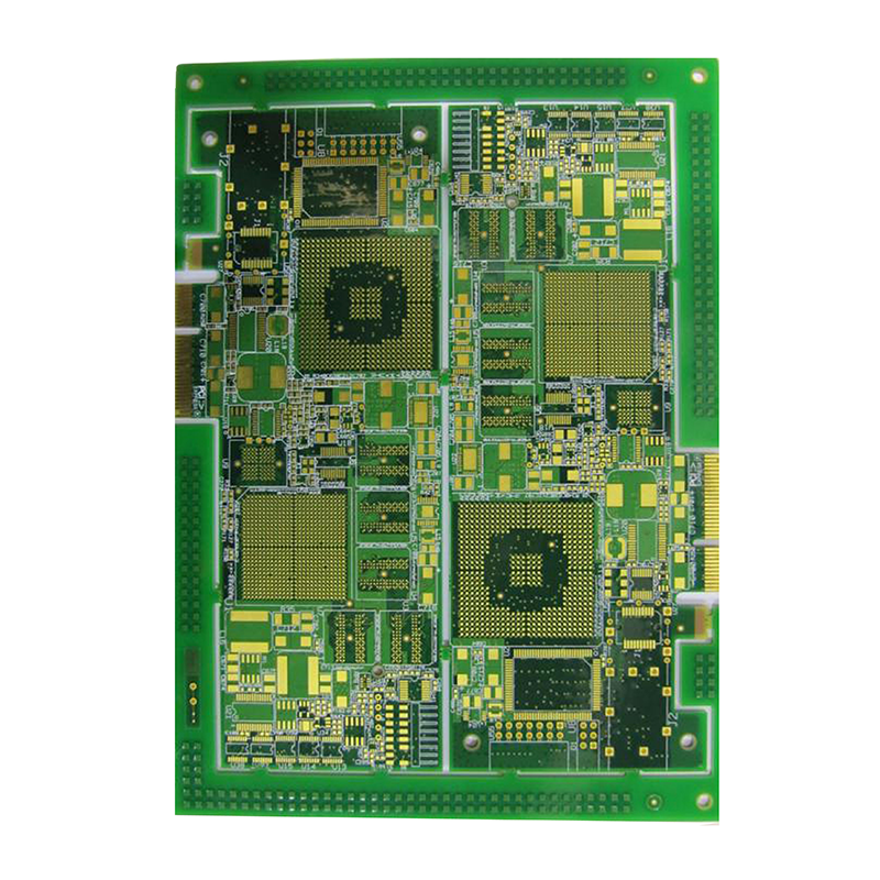
10layer 3 stage HDI Printed circuit board
Layer: 10
Thickness: 2.6 mm
Material: EM-825
Construction: 3+4+3 HDI PCB
Copper: Outer 6 OZ, Inner 2 OZ
Surface: ENIG
Application: Military
Minimum blind/Buried hole: 0.1 mm/0.15mm
Minimum line width: 3.6mil
Line spacing: 3.6mil
Product Details
HDI printed circuit boards are often used in industrial and military fields. This is because they are made of high-quality materials, so they are suitable for use in harsh environments.
What are the advantages of HDI PCB?
1.Excellent functionality: HDI PCB is an ideal choice focusing on weight, space, reliability and performance.
2.Compact design: The combination of blind hole, buried hole and micropore reduces the requirements for circuit board space.
3.Better signal integrity: HDI combines the through hole and blind hole technology in the pad to help place components close to each other, thus shortening the length of the signal path and significantly improving signal integrity.
4.High reliability: The realization of stacked vias makes these PCBs become super shielding against extreme environmental conditions.
5.Economical and efficient: When the density of PCB is increased to more than eight layers, the cost of HDI manufacturing will be lower than that of traditional complex pressing process.