- upload bom file
- +86 0755-82770375
- info@onepcba.com
- Compare Products
- Change Location:
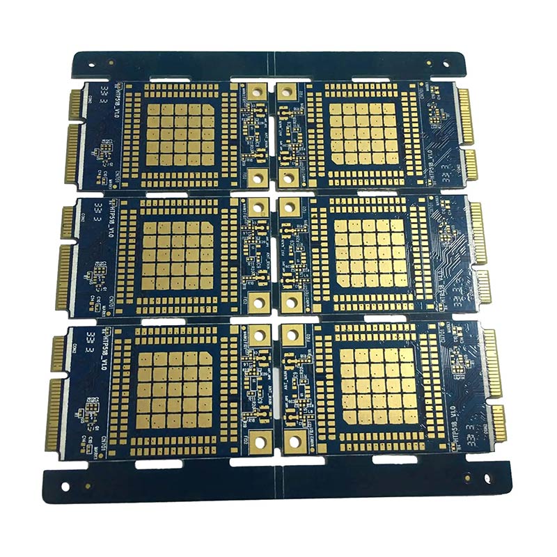
8L 2+N+2 PCB
Layer: 8
Thickness: 2.0 mm
Material: ITEQ 180
Construction: 2+4+2 HDI PCB
Copper: Outer 3 OZ, Inner 5 OZ
Surface: Immersion gold 2U"+ OSP
Application: Communication
Minimum hole: 0.1 mm
Minimum line width: 3 mil
Product Details
HDI PCB can be divided into: 1st, 2nd, 3rd, 4th and any layer interconnection
1-stage HDI structure: 1+N+1 (pressing twice, laser once)
2-stage HDI structure: 2+N+2 (3 times of pressing, 2 times of laser)
3-stage HDI structure: 3+N+3 (4 times of pressing, 3 times of laser)
4-stage HDI structure: 4+N+4 (5 times of pressing, 4 times of laser)
about us
Product And Service
Customer Service
Follow us
Payment