A Real Risk Case in Component Kitting: Recent BGA Issues - Refurbishment, Contamination, and Failed Solderability!
Word Explanation
Solderability Test is a standardized method for evaluating the soldering performance of electronic components. By simulating actual soldering conditions (such as temperature, time, flux action, etc.), it observes the wetting of solder on the surface of pins or solder balls.
In electronic component inspection, the Solderability Test is often regarded as a "basic process", but for devices adopting BGA (Ball Grid Array) packaging, it is a crucial link in assessing reliability.
Today, through the problems found by Onepcba in the testing of BGA samples from different batches of customers' Component kitting recently, we will discuss the importance of solderability for BGA and why the Solderability Test is an indispensable testing link.
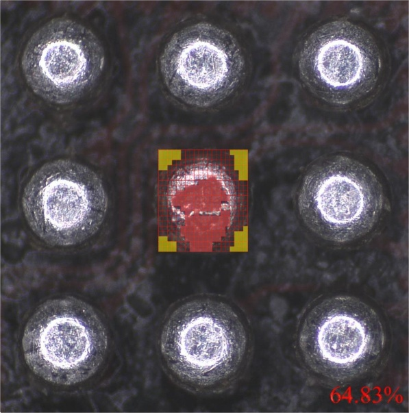
In the first batch of samples, inspectors found obvious contamination and scratches during the External Visual Inspection (EVI) phase.
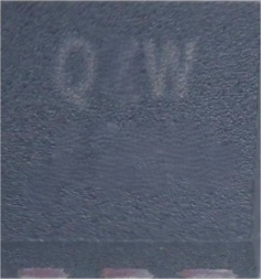
Even without considering soldering performance, the contamination and scratches on the surface of BGA packaging themselves pose potential risks. Contaminants such as grease, dust, or ionic pollution from human contact may lead to increased leakage current or electrical short circuits; if scratches penetrate the metal layer or solder mask, they will damage the insulation protection.
For high-reliability industries such as automotive, aerospace, and medical, even if appearance abnormalities do not directly affect functionality, they may be regarded as signals of abnormalities in the manufacturing or supply chain processes.
At the same time, on the other side of the contamination and scratches, inspectors also found signs of refurbishment.
This means the device may have been used, removed, or exposed to an uncontrolled environment, and then re-entered the market after processes such as re-polishing, cleaning, or reballing.
Such refurbishment behaviors often damage the sealing performance and pad flatness of the original packaging, leading to internal structure damage or uneven heating of pins.
Even if the appearance is "restored", internal microcracks, residual contaminants, or metal fatigue may still cause early failure during use.
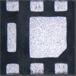
In another batch of BGA test samples, no signs of refurbishment or usage were found.
However, contamination was also found on the solder balls of these samples.
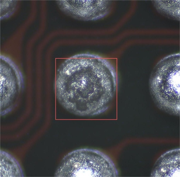
After entering the solderability test phase, a key problem was exposed: some solder balls exhibited poor wetting and insufficient solder spreading, and were ultimately judged as failed.
Failure in the solderability test indicates that the component pins or pads cannot form a reliable metal bond with the solder.
This is usually caused by oxidation, contamination, or plating aging.
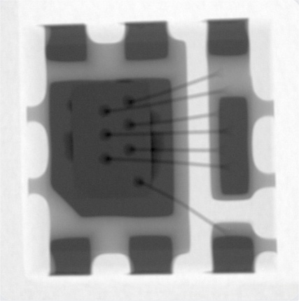
Unlike traditional pin devices, all solder joints of BGA are located at the bottom of the chip, and they can hardly be directly observed with the naked eye after soldering is completed.
This means that once there are hidden dangers in solderability (such as solder ball oxidation, contamination, or deformation), it is likely to lead to the following during the assembly process:
- Cold solder joints: The solder joints seem to be bonded, but there is actually poor contact;
- Bubbles or voids: Reduce electrical conductivity and heat dissipation performance;
- Early failure: Accelerated fracture under high temperature and high stress environments.
These risks often only manifest after the product is put into use, and the resulting rework, recall, or reputation loss far exceeds the testing cost.
Therefore, conducting solderability tests on BGA devices is not only necessary but also crucial.
In the case shared today, the Onepcba laboratory team combined multiple testing methods: External Visual Inspection (EVI) to find surface scratches, contamination, and signs of refurbishment; Solderability Test to verify the wetting of solder balls; and X-ray analysis to detect internal defects of solder balls.
Through comprehensive analysis, it can be judged whether the problem is caused by surface oxidation of some solder balls due to previous use and poor cleaning processes, resulting in insufficient wetting of the metal layer by the solder.
These findings helped the customer trace the problematic link and also reminded that the service requirements of Component kitting are: any slight negligence in storage, transportation, packaging, and even production line switching may lead to subsequent soldering failures.
BGA packaging represents the trend of high-density and high-performance electronic assembly, but it also places higher requirements on surface cleanliness and soldering process control.
With multi-dimensional testing capabilities covering solderability, appearance, X-ray, microscopic analysis, etc., Onepcba helps Component kitting identify risks from the source, ensuring that every link of the device from procurement to assembly is traceable, verifiable, and reliable.
About Us
Onepcba has an ISO17025-accredited laboratory, providing accurate and reliable professional testing. It can objectively and impartially test electronic components, providing true and reliable data and evaluation results for Component kitting buyers.