Blog

TE announces full price increase by 2026, is the "cost storm" of the electronic industry chain coming?

On December 4, 2025, global connector leader TE Connectivity (hereinafter referred to as "TE") issued a price adjustment notice to its global channel partners, announcing that from January 5, 2026, it will implement price increases for all product lines and regions. This is another full line price increase after several rounds of structural price adjustments in the past, covering multiple categories including automotive connectors, high-speed communication connectors, industrial automation connectors, and sensing products.
Against the backdrop of continuously rising manufacturing costs, strong structural demand, and persistent global inflationary pressures, TE's action is not surprising, but it is enough to trigger a shock throughout the entire supply chain. This article will analyze the market signals behind this price increase from three dimensions: the event itself, the logic of the price increase, and the impact on the industry.

1 What are the characteristics of TE's price increase this time?
According to TE's latest channel notification, this price adjustment includes three obvious features:
Effective for all regions: This price adjustment is not just a trial price increase in regional markets. The announcement clearly states that it applies to all authorized dealers and emphasizes "global consistency".
Full product line usage: from automotive connectors to high-speed backplanes, from wire spring terminals to various industrial connectors, with a wide range of price increases. Some categories have received feedback from dealers that the price increase ranges from 5% to 12%, indicating a moderate intensity of structural price hikes.
Resolutely taking action: In the past five years, TE has repeatedly carried out structural price increases during periods of metal price fluctuations and small-scale economic upswings. For example, on December 15, 2021, TE announced a price increase, but the increase was within the range of 5% to 10%, mainly concentrated in high-performance categories. And this time it is' comprehensive coverage ', which means that its judgment on future cost curves and demand structures is very clear.

From a historical perspective, TE's price increases usually have a guiding significance, as it holds a leading position in the global connector industry in terms of market share, technological discourse power, and coverage. This official announcement has given the industry new expectations for the cost trend of connectors in the first half of 2026.

2 Why is there a price increase?
According to the TE price adjustment notice, this price increase is "affected by multiple factors such as inflation and rising prices of metal raw materials".
Global inflationary pressure persists: TE's first reason in the price adjustment letter is "global inflation". According to the "Economic Expert Survey" released by the renowned German think tank Ifo Institute for Economic Research on August 18th, economists from many countries generally predict that global inflation levels will continue to remain in a relatively high range in the coming years. Under inflation, raw materials, labor, and manufacturing services (such as electroplating, stamping, and injection molding) still show varying degrees of increase, especially for large multinational enterprises with global scale production, the cumulative effect of comprehensive costs is very obvious.
Copper prices and precious metal coatings have fluctuated significantly: Since 2025, the operating range of copper prices has significantly increased. On December 8th, Caixin News Agency reported that LME copper prices have expanded, breaking through $11705 per ton and setting a record high. The research report by CITIC Securities predicts that $12000 will become a new starting point for copper prices. The industry chain generally acknowledges that cost pressure is no longer manageable - copper prices have risen by about 10% to 18% within a year; Silver, gold and other precious metal coating materials maintain a high level; The prices of electroplating chemicals fluctuate frequently, with some categories experiencing a 15% increase.

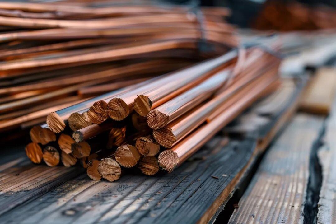
For core components such as terminals, busbars, wire spring components, and shielding parts in connector manufacturing, material prices almost directly determine the cost composition. TE is one of the world's largest users of copper based terminals, and the material end pressure has the power to drive price increases.
International Cable and Connection believes that in addition to inflationary pressures and rising material costs, high-performance demand remains an important driving force for this round of price increases.
From 2024 to 2025, the demand for automotive high-voltage high-speed connectors, AI servers and high-speed data center interconnection, and industrial automation and new energy equipment interconnection will maintain high-speed growth. Its related products have common characteristics such as high specifications, high material costs, difficult delivery, high R&D investment, and limited capacity expansion.
Against the backdrop of supply-demand mismatch, the industry consensus has become that "high-end scarce goods are rising in price". TE has further expanded its price range from high-end to all product categories, essentially reflecting its confidence in future demand intensity and a reassessment of changes in supply and demand structure.

3 What industry impacts may price increases have?
The price increase of industry leaders' products is not just a single brand behavior, but often triggers a systematic response in the global supply chain, especially in the connector industry where TE is located, which is in a special cycle of "high manufacturing costs+rising high-end demand".

More foreign companies follow up with price increases: The industry generally believes that the signal released by this price increase is clear: the global cost side is unlikely to significantly decline in the first half of 2026; The demand for high-performance connectors is still expanding; International giants tend to take collective actions in order to maintain their gross profit structure. Companies such as Molex, Amphenol, and Anbofu may implement partial price increases based on their own product categories, most likely concentrated in high-speed interconnection, automotive high-voltage, and industrial charging products.
In the short term, there is a "rush replenishment" in the inventory cycle: it is still some time before TE officially adjusts prices, but some distributors may place orders with TE in advance and purchase certain key products at prices that have not increased. This is common in the history of TE price increases: 3-4 weeks before the price increase, there is a "replenishment peak"; Demand returns to rationality after price increases; In the medium term, the industry will return to a normal pace. For automotive, industrial control, and power equipment customers with stable demand, such price increases often stimulate "price locking replenishment", especially for models with tight delivery.
Downstream terminal products have entered a new period of cost increase: in the short term, the costs of automotive wiring harnesses, industrial equipment, server machines, and other products will be transmitted. For Tier1 and OEM companies that rely on TE's high-end product system, there is limited room for substitution, and price increases can only be partially absorbed. Especially as car manufacturers are in the stage of accelerating the implementation of electrification and intelligence, the value of connectors per vehicle continues to grow; The demand for AI servers is still high, and high-speed interconnect devices are irreplaceable. Therefore, it is highly probable that downstream price increases or profit margins will be reduced.
Domestic substitution brings structural opportunities: every time an international leader raises prices, it creates a window for domestic enterprises. But the previous domestic substitution mostly stayed at the "expansion of low-end market share", while this time it is "expansion of high-end gap+price increase of international giants". Clear beneficiary direction: high-voltage vehicle standard connectors and wiring harnesses; Industrial automation and energy storage connectors; High speed and medium speed communication connectors; High power and new energy side connection busbar; Special connectors with complex structures and high flame retardant requirements. If domestic enterprises enter a mature stage in reliability, terminal materials, precision molds, and electroplating consistency, they will have more opportunities for Tier 1 certification.

Conclusion
TE's price adjustment notice is like an industry trend forecast: the competition among connector companies in the future will no longer be limited to scale and price competition, but will focus on the comprehensive strength competition of high-performance technology breakthroughs, high material cost control, and high reliability quality assurance.
For the entire interconnection industry, this is not only a survival challenge under cost pressure, but also a strategic opportunity for technological upgrading and market restructuring.


After considering power derating design when selecting resistors, is it still necessary to consider temperature derating design? Many people would answer incorrectly.

After considering power derating design when selecting resistors, is it still necessary to consider temperature derating design? Many people would answer incorrectly.

Typically, the rated power of a resistive component is determined under specific operating conditions, including ambient temperature and current flow. However, since resistive components are affected by various factors in actual operation, such as changes in ambient temperature and fluctuations in current flow, it is necessary to appropriately reduce the rated power to ensure that the resistive component can operate reliably under all operating conditions. Therefore, when selecting resistors, we need to consider that the rated power and actual temperature of the resistor do not exceed the maximum operating range allowed by the specifications. This derating is to ensure that the resistive component does not overheat and fail during long-term operation.

1. Power Derating
For surface-mount resistors, 70°C is generally the critical temperature point for power derating.  This is especially important to consider when the operating temperature of the resistors in your product exceeds 70°C. It's important to note that different manufacturers use different reference temperature points for their derating curves. For example, KOA's surface-mount resistor specifications provide two derating curves: one based on ambient temperature and the other on terminal temperature.  The choice depends on your specific application. If you are unsure whether to use the rated ambient temperature or the rated terminal temperature, prioritize the rated terminal temperature. The actual maximum power at which the resistor operates must be less than the power value corresponding to the derating curve.

2. Temperature Derating
Different resistors have specific operating temperature ranges. The actual operating temperature of a resistor must not exceed the maximum temperature limit specified in the datasheet. So, how is the resistor's operating temperature calculated?
Resistor temperature = Ambient temperature + Resistor temperature rise. The ambient temperature is the operating environment temperature of the product. Considering the extreme case, this would be the maximum operating ambient temperature. The resistor temperature rise can be obtained through calculation, i.e., temperature rise = thermal resistance * power. It can also be obtained through temperature rise testing.

For example, when selecting a resistor, if a resistor has a rated operating power of 0.5W and a maximum operating ambient temperature of 120°C, and it operates at 0.25W, assuming a temperature rise of 20°C, should the power derating be considered based on the derating at 120°C or 140°C? Many people think it should be considered based on the derating at 140°C because the final temperature of the resistor is 140°C. If you think this way, you are wrong, because power derating itself already takes into account the temperature rise of the resistor. Therefore, considering the temperature rise again before performing power derating is equivalent to derating twice, which is over-designing.

Even though a 1% precision resistor was selected for voltage divider sampling, the resistor's accuracy exceeded 1% after mass production. The issue isn't with the resistor itself—it turns out to be

Many hardware engineers often only consider whether the resistor's tolerance is F or J when selecting resistors, which can sometimes lead to significant issues. Tolerance is one of the key parameters of a resistor. So, how should we consider the tolerance when selecting resistors? It depends on the specific role the resistor plays in the circuit. Resistors generally serve two primary functions:

The function of resistor 
1. Current limitation: Resistors regulate the current in a circuit by limiting the flow of current. For example, a voltage regulator diode generally requires a series resistor and cannot be directly connected in parallel with a power supply.
2. Voltage divider: Resistors can be used as voltage dividers in circuits. For example, if we want to collect a certain voltage signal, we need to use resistor voltage division to convert the voltage signal into a voltage range that the MCU's ADC can accept.

When the function of a resistor is to limit the current, the accuracy of the resistor is generally not that important. When calculating WCA, we only need to confirm that the resistor at the lower limit of the resistance value will not cause the current in the circuit to exceed the limit value, because high-precision resistors are generally more expensive. In this case, we can choose a conventional 5% precision resistor. When the function of a resistor is to divide voltage, assuming our goal is to accurately collect voltage signals, we generally need to use resistors with an accuracy of 1% or even 0.1%, because the error of the resistor will affect the value of the voltage signal divided by the resistor network.

What factors can affect the accuracy of resistance?
1. Manufacturing tolerance resistors involves laser cutting during production, which involves measuring the resistance value of each resistor body and using laser cutting to form the target resistance value. Generally, the initial value of batch production of surface mount resistors is smaller than the target resistance value. At this time, by adding cutting technology to the resistor body to narrow the current path, the resistance value will increase. After laser cutting, it will be within the resistance error range specified in the resistance specification book.
The accuracy of resistors is represented by corresponding codes, such as F representing ± 1% and J representing ± 5%. However, it should be noted that the accuracy error values corresponding to the accuracy codes only include manufacturing tolerances and do not include accuracy deviations caused by other factors.

2. The temperature coefficient resistance value actually changes with temperature. The resistance specification book will include an indicator called the Temperature Coefficient of Resistance (TCR), which represents the relative change in resistance value when the temperature changes by 1 degree Celsius, measured in ppm/℃. Temperature coefficient of resistance=(R-Ra)/Ra ÷ (T-Ta) × 1000000; Among them, Ra represents the resistance value under the reference temperature condition, usually at room temperature of 25 ℃, Ta represents the reference temperature, usually at room temperature of 25 ℃, R generally represents the resistance value of the resistor under a certain temperature condition in the product, and T is the corresponding temperature. We usually use this formula to calculate the resistance deviation of a resistor at the upper or lower temperature limit of the product application environment.


For example, suppose the TCR of a chip resistor is 100ppm/℃, the reference temperature is 25 ℃, and the actual temperature upper limit of the resistor is 125 ℃. So, what is the resistance change rate of the resistor at 125 ℃?
(125-25)*100/1000000=1%。
Through the above calculations, we found that the resistance change rate of the resistor at 125 ℃ reached an astonishing 1%. If the manufacturing tolerance of the resistor is 1%, the impact of temperature on the accuracy of the resistor cannot be ignored. So when calculating the deviation of resistance value, it is necessary to consider the influence of temperature, especially when collecting voltage or current signals, otherwise the consequences will be very serious.

EDA Software Development Engineer: The Pathfinder for Semiconductor Chips

EDA Software Development Engineer: The Pathfinder for Semiconductor Chips

EDA Engineers: The Unsung Warriors Powering the Chip Industry

EDA is often hailed as "the invisible warrior standing behind chips, wielding the sword for all."
"Without EDA, the chip industry is like a general without a map or a soldier without weapons."
Yet the reality is: While chip designers race to meet endless deadlines, EDA engineers—Chase the deadline of an entire industry.
Others only see your back as you code,But only you know,Every feature you build saves thousands of design engineers time, mitigates risks, and boosts success rates.
EDA engineers don’t just develop tools;They pave the way for the future of chip design.

I. The World of EDA: A Deep Dive Few Enter, and None Easily Exit

Every EDA engineer undergoes these phases:

1. Entry Stage:

You think you’re coding—turns out you’re wrestling with math, physics, and algorithms.
When others add features with simple code, you need to master:
  • Logic synthesis
  • Placement and routing (P&R)
  • Device modeling
  • Parasitic extraction
  • Algorithms, graph theory, and optimization
  • Parallel computing and data structures
Many newcomers sigh:"I thought I was becoming a software developer, only to realize I need to relearn every discipline."

2. Mid-Career Stage:

You think you’re implementing features—instead, you’re trapped in the hell of performance optimization.
EDA software processes data with millions, tens of millions, or even hundreds of millions of nodes.Optimizing algorithm complexity from O(n²) to O(nlogn) to O(n) isn’t optional—it’s mandatory.
You’ll experience:
  • Waiting 30 minutes for a single run after modifying one function;
  • Earning company-wide praise for optimizing a data structure;
  • Holding up dozens of design engineers when your tool lags.
Finally, you understand:"In EDA software, 0.1 seconds is a matter of life and death."

3. Senior Stage:

You think you’re building tools—actually, you’re shaping a company’s tape-out success rate.
As more people use your tools, you realize:Your bugs are never just bugs.
They can cause: DRC violations missed in layouts, timing closure failures, simulation discrepancies, yield anomalies…
You come to recognize:"I’m not just a developer—I’m the invisible guardian of the entire chip team."

II. The Pains of EDA: Unseen Fatigue and Heavy Responsibility

1. Your Code is a Lifeline for Others

A DRC tool missing a violation?— Tape-out fails catastrophically.A P&R router going off-track?— The entire project grinds to a halt.A simulator producing inconsistent results?— Everyone questions their work.
You may only modify a few hundred lines of code,But it impacts multi-million-dollar projects.
You dare not submit casually:You run dozens of regression cases before a patch;You stare at a single line of code for 30 minutes before committing.
Because you know:"The reliability of EDA tools is the backbone of countless engineers."

III. The Achievements of EDA: Pride Unknown to Others

You grow accustomed to moments without thanks:
  • You optimize a parser, making all tools 20% faster—no one knows it’s your work;
  • You fix an obscure bug, and only one team notices the difference;
  • Your algorithm reduces routing by 10,000 wires—only the silent yield curve proves you’re right.
But one day, you’ll hear:"A CE from a major firm says, ‘Your tools are far more stable now.’""A design engineer says, ‘Your latest version finally doesn’t lag.’""A client says, ‘Your algorithm is incredibly intelligent.’"
In that moment, you’ll feel:"Though no one sees me, my code leaves traces across the chip world."

IV. EDA Engineers: Masters of Breaking Down Complexity

You gradually get used to:
When asked, "Can this feature be implemented?"You reply, "Let me first see if math has a solution."
When asked, "Can we make it faster?"You reply, "Let me battle time complexity."
When asked, "Why are the results inconsistent?"You reply, "Let me check the logs—then the logs of the logs."
You learn to "see the essence of systems"—that’s growth.
EDA’s core isn’t code; it’s turning the impossible into controllable, and complexity into simplicity.

V. The Romance of EDA Engineers: Unspoken Persistence

Others see you:
Coding late into the night,Tweaking algorithms till dawn,Staring at memory usage curves like they’re your stock portfolio,Drinking cold coffee in front of the terminal,Chasing a segmentation fault for two days straight,Writing dozens of test cases for one timing corner.
Only you know:You’re not just building tools—You’re laying the foundation for the entire chip industry.
"You write code, but you prop up an industry.""Others press buttons; you invest your youth."

VI. A Message to All EDA Software Development Engineers

If you’re currently:
Tormented by performance bottlenecks,Driven crazy by multi-thread scheduling,Doubting your sanity over a corner case,Frustrated enough to throw your computer at user demands,Staring at a page full of red FAILED regression results—
Remember:You’re doing the most fundamental, critical, and hardcore work in the industry.Your value isn’t measured by lines of code per day, but by the "possibilities" you create for thousands of chip engineers.
A final golden quote for you:"Without EDA, there are no modern chips;Without you, there is no EDA."
"You are not just tool authors—you are the cornerstone of the chip era.""In the shadows, you strive to make the future computable."
Salute to all EDA engineers—The quietest, most resilient, and most respectable engineers in the chip world.
"China's First Production of Solid-State Batteries: Accelerated Breakthrough of Domestic Industrial Components in China"

All-Solid-State Battery Industrialization Enters Acceleration Phase: Core Advantages, Industrial Chain Opportunities, and Key Challenges

Recently, China's first high-capacity all-solid-state battery production line, constructed by GAC Group, has been officially completed and commenced small-batch test production. This breakthrough marks the transition of all-solid-state batteries—once regarded as a "laboratory concept"—into a new phase of industrial application. For the electronic components industry, this technological innovation not only signifies the iteration of batteries themselves but also will trigger in-depth transformations across the entire industrial chain, from materials and equipment to upstream and downstream applications, bringing a new wave of development opportunities to the industry.

Core Advantages and Prospects of All-Solid-State Batteries

Compared with traditional lithium-ion batteries, the core advantage of all-solid-state batteries lies in their entirely solid-state composition without any liquid electrolytes. This fundamental transformation stems from two key technological innovations:
  1. Anode Manufacturing: A new dry-process integrates three traditionally independent steps—slurry processing, coating, and calendering—into a streamlined workflow, significantly reducing energy consumption and improving production efficiency.
  2. Electrolyte Technology: The production line abandons conventional liquid electrolytes in favor of independently developed solid electrolyte materials, which can withstand temperatures exceeding 300-400°C—far surpassing the 100°C+ limit of liquid electrolytes—thus achieving a fundamental improvement in battery safety.
From the perspective of the electronic components industry, the completion of all-solid-state battery production lines will first drive a surge in demand for solid electrolyte materials. As the core material of all-solid-state batteries, the performance of solid electrolytes directly determines battery energy density and safety. Domestic enterprises have already achieved breakthroughs in independent R&D, successfully replacing traditional liquid electrolytes. With the commissioning and mass production of production lines, demand for solid electrolytes will grow rapidly, benefiting related material R&D and production enterprises through industrial scale expansion.
Upstream in the industrial chain, all-solid-state batteries impose higher requirements on raw materials such as electrode materials and copper foil (e.g., high areal capacity electrode materials and ultra-thin copper foil). Some enterprises have already achieved mass supply of key raw materials for solid-state batteries. As production capacity is released, upstream raw material manufacturers will face a market environment of rising volume and prices, with industrial chain synergy effects gradually emerging.

Opportunities and Challenges in the Industrial Chain

The battery manufacturing equipment sector is also embracing new industrial opportunities. Due to the significant differences in production processes between all-solid-state batteries and traditional liquid batteries, new technologies such as dry-process anodes have driven a comprehensive upgrade of production equipment, creating a demand for modification or replacement of existing wet-process equipment. Equipment manufacturers with technological reserves and capacity layout in specialized equipment fields—such as dry-process electrode preparation and solid electrolyte coating—will witness expanded market demand and broad growth prospects.
For example:
  • Laser welding and cleaning equipment provider Lanying Laser has already captured this trend, with its product portfolio covering laser welding, cleaning, and gluing equipment. It has secured hundreds of millions of yuan in orders for semi-solid-state battery equipment and began receiving orders for all-solid-state battery equipment last year.
  • Leading Intelligent, the world's only supplier of full-process solid-state battery equipment, reported a 210% year-on-year surge in solid-state equipment revenue in Q1 2025, demonstrating strong growth momentum. This fully indicates that the construction of all-solid-state battery production lines is injecting robust impetus into the electronic equipment manufacturing sector.
Despite broad prospects, the industrialization of all-solid-state batteries still faces numerous challenges. Wan Gang, Chairman of the China Association for Science and Technology, stated in a recent speech that while all-solid-state batteries have entered the phase of gigawatt-scale pilot line construction, industrialization is hindered by three key bottlenecks:
  1. Material Innovation: Sulfide electrolytes react easily with air, oxide electrolytes suffer from high interface impedance, and polymer electrolytes have low energy density—there is currently no "all-round material" that addresses all issues.
  2. Process Breakthroughs: The yield rate of key processes such as dry-process electrode coating uniformity and solid electrolyte film density remains below 30%.
  3. Cost Dilemma: Current production costs of all-solid-state batteries are 3-5 times higher than those of liquid batteries, requiring cost reduction through large-scale production and supply chain restructuring.
These challenges precisely point the way for technological innovation in the electronic components industry, with substantial R&D potential waiting to be tapped in areas such as material formulation, process control, and cost optimization.

Clear Industrialization Timeline

With a clear industrialization roadmap—small-batch vehicle-mounted testing to start in 2026, and gradual mass production to be achieved between 2027 and 2030—the commercialization of all-solid-state batteries has become irreversible.
In terms of application scenarios, all-solid-state batteries will first be deployed in high-end new energy vehicles, eVTOL (electric vertical takeoff and landing) aircraft, energy storage, and consumer electronics. Particularly in the eVTOL sector, where requirements for battery energy density and safety are extremely high, all-solid-state batteries are expected to take the lead in achieving large-scale mass production.
For the electronic components industry, this trillion-yuan market track is accelerating its opening. Leading enterprises that have proactively laid out in core technology sectors have already gained a first-mover advantage, as an industrial transformation wave driven by all-solid-state batteries sweeps across the industry.
Dutch officials cancel China visit! What is the current status of Nexperia?
New Developments Emerge in the Nexperia IncidentAccording to Dutch media including De Telegraaf and Reuters, Dutch Minister of Economic Affairs and Climate Policy Micky Adriaansens stated on December 2 (local time) that she has canceled her scheduled visit to China in December due to discrepancies in the two sides’ schedules. Reports indicate Adriaansens originally planned to travel to China to hold further consultations on resuming chip supplies and so-called "security issues."
By reading this article, you will learn: What are the latest changes in the Nexperia incident? How is the spot market performing now?
Source: Dutch Government Official Website

01 Latest Updates on Nexperia

On December 2 (local time), Dutch Minister of Economic Affairs and Climate Policy Micky Adriaansens sent a letter to the Dutch Parliament, announcing the cancellation of her planned December visit to China due to scheduling conflicts.
In the letter, Adriaansens noted that while the visit is temporarily canceled, she will travel to China in the near future if the situation regarding Nexperia warrants it, with a new date yet to be determined. She also wrote: "I have reached a consensus with the Chinese side on this matter."
Adriaansens is expected to attend a debate on the Nexperia incident at the Dutch Parliament on December 4 (local time). The debate was arranged at the explicit request of the Parliament, scheduled ahead of Adriaansens’ original visit date to China.
Source: Dutch Government Official Website
Additionally, Reuters reported that Adriaansens included a timeline of the Dutch government’s takeover of Nexperia on September 30 in her letter.
The timeline shows Adriaansens first learned of issues at Nexperia on September 18, when she received information that the company’s then-management had "advanced significantly" plans to relocate operations to China—an action she claimed poses a threat to Europe’s economic security.
Adriaansens made a preliminary decision to intervene on September 25 but only notified the UK, Germany, the US, and China after the intervention was actually implemented.
Below is a summary of recent information released by official sources and authoritative media since the Nexperia incident:
  • November 1: China announced export exemptions for eligible Nexperia products.
  • November 2: Nexperia China issued an announcement to customers stating that Nexperia BV (Netherlands) had unilaterally suspended wafer supplies to its Dongguan assembly and testing facility (ATGD) effective October 26, 2025.
  • November 7 (local time): The Dutch government stated that China would soon resume chip supplies.
  • November 8: China agreed to a request from the Dutch Ministry of Economic Affairs to send a delegation to China for consultations.
  • November 13: According to a report by Jiemian News, automotive industry officials revealed that Nexperia’s Dutch subsidiary had not been shipping silicon wafers to its Chinese subsidiaries for assembly.
  • November 13: In an interview with The Guardian, Adriaansens expressed "no regrets" about the Dutch government’s decision to take over Nexperia on September 30.
  • November 14: Adriaansens announced that a Dutch government delegation would travel to China "early next week" to seek a resolution to issues related to Nexperia, a subsidiary of Chinese company Wingtech Technology.
  • November 14: China’s Ministry of Commerce responded to Adriaansens’ remarks in the interview, stating: "China expresses extreme disappointment and strong dissatisfaction with such remarks that confuse right and wrong, reverse black and white, and act arbitrarily." The Dutch Ministry of Economic Affairs declined to comment the same day.
  • November 19: Adriaansens posted a statement on social media platform X, announcing the "suspension of intervention in Nexperia."
  • November 19: Wingtech Technology issued an announcement stating that its control over Nexperia remains restricted.
  • November 19: China’s Ministry of Commerce stated: "China welcomes the Netherlands’ decision to proactively suspend the administrative order on Nexperia, viewing it as a first step in the right direction toward a proper resolution. However, there is still a gap in addressing the root causes of volatility and disruption in the global semiconductor supply chain."
  • November 20: Wingtech Technology released a "Statement on the Suspension of the Dutch Ministry of Economic Affairs’ Administrative Order" via its official WeChat public account. The statement noted that while the administrative order has been suspended, the emergency measures issued by the Enterprise Chamber of the Amsterdam Court of Appeal (Netherlands) remain in place. The Dutch Ministry of Economic Affairs is obligated to fully and comprehensively resolve the Nexperia issue, and Wingtech’s legitimate control rights and complete shareholder rights as an investor must be restored.
  • November 23: Wingtech Technology released another statement via its official WeChat public account, urging "Nexperia Netherlands to Earnestly Respond, Communicate, and Resolve the Control Issue to Safeguard Global Supply Chain Stability." The statement emphasized that Nexperia Netherlands’ unilateral actions have posed potential threats to the stability of the global semiconductor industry chain. Wingtech called on Nexperia Netherlands to propose constructive and sincere solutions to restore Wingtech’s legitimate control and shareholder rights based on facts and law.
  • November 26: China’s Ministry of Commerce stated that the Netherlands’ improper administrative and judicial interventions in Nexperia have not yet been fully lifted.
  • November 27: Nexperia BV released an "Open Letter to the Leadership of Nexperia’s Chinese Entities" on its official website, stating that Nexperia "remains committed to constructive cooperation with its Chinese entities and has consistently requested open dialogue to find a path forward for resuming normal supplies." Regrettably, the company added, "Nexperia has not received any substantive response."
  • November 28: Wingtech Technology issued an "Official Statement on the Nexperia Control Dispute and Global Semiconductor Industry Chain Stability" via its WeChat public account. The statement criticized Nexperia Netherlands’ November 27 open letter, claiming it contained "numerous misleading false allegations and misinformation," reflecting "a lack of sincerity in resolving the issue by shirking responsibilities and evading key problems." Wingtech emphasized its solemn commitment to addressing the matter.

02 Changes in the Chip Spot Market

A recap of recent trends: Since November, the global chip spot market has generally stabilized, with most participants adopting a wait-and-see approach in the early weeks. Last week, the market remained quiet but saw subtle shifts: available inventory increased (particularly for batches with a production date of 2540+), demand persisted but at lower acceptable prices, and most transactions were driven by foreign trade orders—with some distributors reporting a rise in demand compared to the 观望 period.
For detailed reasons behind the market’s calm regarding Nexperia chips, refer to the recommended reading at the end of this article.
Previously, some large-scale traders continued selective restocking, leading to divergent transaction trends across different part numbers: individual models maintained high prices, while other distributors noted that quotes for some chips had fallen back to historical levels. Market quotes were fragmented, with significant gaps between asking prices and transaction prices. Meanwhile, agents reported that order demand had been somewhat suppressed due to price hikes by original manufacturers.
This week’s chip spot market conditions are largely unchanged from last week, with demand gradually recovering following the wait-and-see phase. Overall demand remains significantly lower than during the peak boom period, but transactions are still occurring—primarily driven by foreign trade. While transaction prices have declined, some part numbers continue to command high prices, and market interest remains strong.
Distributors have reported mixed experiences:
  • Some traders note that demand remains weak, believing that only specific high-demand part numbers present opportunities in the current market.
  • Those focusing on large-scale foreign trade clients report a decrease in demand this week.
  • Distributors with advantageous Nexperia inventory report robust transaction volumes over the past two weeks, with some indicating stronger demand this week compared to last.
Synthesizing current information, the overall market situation has not changed significantly from last week. While the Dutch government’s suspension of the "ministerial order" has eased short-term tensions, the earlier administrative and judicial interventions against Nexperia have not been fully lifted, and the core issue of wafer supply remains unresolved. Market sentiment is gradually shifting from wait-and-see to recovery, with prices and transactions showing divergent trends.
The Intricate Scheme Behind Memory Chips: Market Trends & Technical Insights

The Intricate Web of Memory Price Surge

In October 2025, OpenAI signed an agreement with Samsung and SK Hynix under the project name "Stargate", securing a monthly supply of up to 900,000 DRAM wafers. This volume accounts for roughly 40% of the global DRAM output, which was snapped up entirely by a single buyer. The deal is part of OpenAI’s four-year, $500 billion infrastructure development initiative. Every observer of the memory market could easily foresee the subsequent market trends.
Following the announcement of the deal, the price of contracted DRAM soared by 171%, while the impact on the retail market was even more drastic. A set of Team Delta RGB 64GB DDR5-6400 memory modules was priced at $190 in August; now, the same product is listed online for $700. In less than three months, the price has surged by a staggering 268%. Such a steep price hike is almost unprecedented in the commodity markets during peacetime. Even the price of DDR4, which was supposed to be in oversupply, more than doubled.
Storage devices were also hit hard. Western Digital’s WD Blue SN5000 1TB SSD rose from $64 to $111, and the 2TB version climbed from $115 to $154. Demand is only part of the equation. OpenAI’s "Stargate" expansion requires enormous amounts of High-Bandwidth Memory (HBM). Data centers and consumer electronics manufacturers are competing for the same basic resources, with the former offering much higher prices—far higher.
Factories are redirecting their advanced DRAM production capacity toward AI-related needs, as the quotes offered by data centers are unmatchable by consumer device manufacturers. The situation might have been manageable if the supply had remained stable, but unfortunately, that was not the case. Samsung, SK Hynix, and Micron have all shifted their production lines to HBM, a specialized high-bandwidth memory designed for AI accelerator chips, where profit margins are significantly higher than those of consumer-grade DDR5. Micron’s entire HBM production capacity for 2026 has already been fully booked.
Despite continued purchases by PC manufacturers, the production volume of wafers for traditional memory modules keeps declining. What we are witnessing, therefore, is a surge in demand coupled with a restructuring of production. This indicates that the intricate collusive scheme behind the memory price surge has evolved into a predicament with no short-term solutions.
This memory market cycle differs from previous ones in that the upgrade path of AI infrastructure is drastically distinct from that of consumer hardware. Once these data centers are completed, they will continuously consume massive amounts of memory as AI models scale up, resulting in an ever-upward trending demand curve.
In the face of this market upheaval, tech giants have responded in vastly different ways, splitting themselves into two distinct camps. Sony stockpiled ample memory supplies for the PlayStation 5 before prices skyrocketed. According to industry insiders, its inventory is sufficient to maintain stable console prices for months to come and may even help the company weather the entire shortage period unscathed.
Apple also secured its supply in advance, and its profit margins are robust enough to absorb such cost increases that would cripple low-margin businesses. Lenovo went a step further: Bloomberg reported that its memory inventory is approximately 50% above the normal level, enough to sustain its operations until 2026.
In contrast, Microsoft finds itself in a passive position. Industry analysts predict that the Xbox console will most likely face another price hike, following an increase earlier this year. Valve’s timing could not have been worse. The core component costs of its highly anticipated living room gaming PC, the "Steam Machine", were two to three times higher than everyone’s budget by the time of its launch. The company refused to confirm the final retail price and directly attributed the issue to the memory shortage. Any value proposition it had planned was completely undermined by soaring memory costs. Framework, a modular laptop manufacturer, has removed all standalone memory modules from its online store.
The divide between these camps, shaped by their foresight, is exerting a profound impact on the competitive landscape—effects that will linger even if prices stabilize in the future. Sony and Lenovo have maintained their market positions, while Microsoft and Valve have fallen victim to the crisis. Effective supply chain management over just a few months has condensed market share shifts that would typically take years to unfold.
A natural question arises: as Samsung, SK Hynix, and Micron watch memory prices triple, why don’t they ramp up production to capitalize on the profits? Anyone who experienced the 2018 oversupply crisis would have a definitive answer.
From late 2016 to early 2017, tight memory supply pushed prices upward. The three major manufacturers responded by breaking ground on new wafer fabs in South Korea and China and expanding production capacity at existing facilities— a straightforward response on paper. Chasing high prices to boost capacity seemed logically sound in theory. However, the strategy collapsed in 2018. Demand plateaued just as all the new production capacity came online simultaneously, leaving warehouses overflowing with unsold chips.
Samsung’s semiconductor division, once a reliable profit engine, reported quarterly results that shocked investors. SK Hynix fared no better. The shadow of oversupply loomed until 2019 before gradually lifting. This bitter experience has profoundly shaped every production decision these companies make today.
Building a memory wafer fab and bringing it into operation takes years. Wafer allocation decisions made in November 2025 will determine market supply in 2027 and even 2028. Yet no one can predict whether AI infrastructure investment will remain as robust by then. What if the development of Artificial General Intelligence (AGI) hits a bottleneck? What if hyperscale users realize they have overinvested and start canceling orders?
Manufacturers would rather maintain the current shortage than repeat the disaster of oversupply. They call this "discipline", though consumers—who have watched $89 memory modules jump to $310—would likely use harsher terms.
Industry forecasts indicate that the tight supply of DRAM and NAND will persist until 2026, with only cautious optimism about a return to normalcy in 2027. Backlogs for large-capacity nearline hard disks already extend two years into the future, and distributors have begun bundling memory modules with motherboards to control inventory allocation.
Taking a broader view, an unsettling reality emerges: PC builders and gamers are essentially funding the development of AI infrastructure. Not directly or voluntarily, but this is precisely how the mechanism operates. Hyperscale users including OpenAI, Microsoft, Google, and Amazon have driven up memory prices to stock up for their training clusters. Manufacturers prioritize fulfilling these large orders, resulting in shrinking availability in the retail market. A teenager saving up for a gaming PC now has to pay an extra $400 for memory that cost only $130 three months ago.
There has never been a public policy debate weighing whether accelerating AI development is worth the cost of rising consumer computing expenses. The market simply allocates resources to the highest bidder—and when a single buyer can lock up 40% of global supply, this process becomes rapid and brutal.
Nearly all of the world’s DRAM is produced by just three companies. This high level of concentration has created systemic vulnerabilities that have not received adequate regulatory attention. Frankly speaking, the time has come to re-examine this situation.
[Risk Case Study] A Transaction Involving "High-End Memory" Reveals Supply Chain Crises

[Risk Case Study] A Transaction Involving "High-End Memory" Reveals Supply Chain Crises

In the global semiconductor supply chain, the risk of counterfeit electronic components is never far away—even in critical links like Component Kitting, where pre-assembled component sets are prepared for manufacturing or procurement. According to the latest case released by ERAI, a supplier has been listed on the high-risk supplier list on suspicion of providing counterfeit components in transactions, a breach that could have severe ripple effects if the fake parts had entered Component Kitting processes downstream.
Today, we share this real case to shed light on the hidden crises behind these seemingly "cost-effective" transactions, especially how counterfeits can infiltrate and disrupt Component Kitting and subsequent production workflows.

Cause: An Unexpected Email

Recently, a U.S. buyer received two unsolicited emails from a supplier claiming to offer various well-known brands of electronic components—including laptop computers, storage devices, memory modules, and parts commonly used in Component Kitting.
Tempted by the favorable price and delivery time (terms often used to lure buyers into cutting corners in Component Kitting sourcing), the buyer placed an order for Samsung memory modules worth over $10,000, made the payment online, and agreed on delivery within one week. These modules were initially intended to be integrated into the buyer’s Component Kitting for downstream device assembly.
(Image for reference only)Reminder: Using third-party payment platforms or personal accounts for high-value transactions—whether for standalone components or Component Kitting materials—is often a red flag.

Apparently "Qualified," but Flaws in Details

After receiving the goods, the buyer’s initial tests showed the memory modules "could work," but there were some "defects" in their appearance—red flags that would have been easy to overlook if the parts were rushed into Component Kitting without thorough inspection.
Further inspections uncovered more issues that would have compromised any Component Kitting process using these parts:
  • These memory modules, labeled as brand-new (a standard requirement for most Component Kitting to ensure product consistency), actually had obvious signs of use, with torn or replaced labels;
  • Professional memory testing equipment revealed that the SPD data of these modules had all been tampered with to match the model and date code on the labels— a deception that could go undetected in basic Component Kitting pre-checks;               
(Image for reference only)
  • Some 32GB 2933 modules were "disguised" as 32GB 3200— a mismatch that would cause performance failures if integrated into Component Kitting for high-speed devices;
  • More seriously, 64GB Load Reduced modules were passed off as Registered modules, but the abnormal layout of additional chips was clearly distinguishable through visual inspection. This mix-up would not only disrupt Component Kitting compatibility but also lead to equipment malfunctions post-assembly.
This means the products were not the high-specification memory they claimed to be, but rather "substandard" refurbished or counterfeit parts—risky additions to any Component Kitting process that demands reliability.

Knowledge Point: What is SPD Tampering?

SPD (Serial Presence Detect) is a chip that stores module information, a critical data source for verifying component compatibility in Component Kitting.
By modifying the SPD, the system can be "tricked" into believing the memory has higher specifications— a falsification that bypasses basic software checks and poses a major threat to Component Kitting accuracy, as the mismatched parts may not function with other components in the kit.
This counterfeiting method cannot be detected by ordinary software and requires professional equipment and visual inspection for identification— steps that are essential in Component Kitting quality control but often skipped to save time or cost.

Potential Risks: From Blue Screens to   s

Test results indicated that these counterfeit memory modules could not operate at the speed marked on their labels. If these parts had been incorporated into Component Kitting for devices like servers or industrial controllers, the consequences would have been far-reaching:
For example, 2933MHz modules could not safely run at 3200MHz. Forced overclocking (a side effect of mismatched specs in Component Kitting) may lead to:
  • System blue screens and frequent crashes, disrupting operations dependent on the kitted devices;
  • Circuit damage caused by memory overheating, which could spread to other components in the Component Kitting and render the entire kit useless;
  • Even fires in extreme cases, posing safety risks to workers and facilities handling the kitted products.
 
(Image for reference only)It is evident that this not only results in economic losses from wasted Component Kitting materials and rework but also poses more serious safety hazards and reputational damage for businesses relying on the kitted components.

Return? Impossible!

After discovering the issues— which would have made the modules unfit for Component Kitting— the buyer immediately rejected the goods and requested a return and full refund.
The seller agreed verbally, but U.S. law clearly stipulates that once a product is deemed a "suspected counterfeit," it shall not be returned to the supply chain— a regulation designed to prevent fake parts from re-entering Component Kitting or other critical workflows.
Subsequently, the seller refused to cooperate with the refund and completely cut off communication. Further investigations revealed red flags that would have alerted vigilant Component Kitting managers:
  • The company address listed on the seller’s website did not match the actual shipping address, which was actually a residential property— an unusual setup for a supplier of Component Kitting -grade components;
  • The seller claimed to be an authorized agent of well-known brands (a key credential for Component Kitting sourcing), but no authorization records were found through official brand website checks;
  • The seller could not provide any supply chain traceability documents— a must-have for verifying component origins in Component Kitting to avoid counterfeits.
Ultimately, the company was listed as a high-risk supplier by ERAI, warning other businesses— especially those involved in Component Kitting— to avoid partnering with them.

What Can We Do?

This case reminds us that even products with seemingly intact appearances may hide significant risks— risks that are amplified in Component Kitting, where a single counterfeit part can invalidate an entire pre-assembled set. Ordinary testing software and functional verification are insufficient to identify counterfeit parts, especially when integrated into Component Kitting alongside other components.
As an independent third-party laboratory, White Horse Labs operates five ISO/IEC 17025-accredited laboratories worldwide, offering one-stop services tailored to Component Kitting safety: from EVI (Early Vendor Inspection) and X-ray tests to electrical performance evaluations, we help verify component authenticity and compatibility before they enter Component Kitting processes. Our services assist clients in preventing counterfeit components from infiltrating Component Kitting and subsequent supply chain links, ensuring trust and compliance in the complex global procurement landscape.
A single small transaction not only caused losses exceeding $10,000 but also exposed major hidden dangers in Component Kitting and broader supply chain sourcing.
Faced with global procurement and an ever-changing market environment, prioritizing rigorous inspection— especially for Component Kitting materials— is a necessary lesson for every industry professional.
Kind Reminder: If you suspect the quality or authenticity of components intended for Component Kitting or received products, please contact our testing team. Let us work together to safeguard the safety, reliability, and efficiency of Component Kitting and the entire supply chain.

Translation & Keyword Integration Notes:

  1. Strategic Keyword Placement: "Component Kitting" is embedded in contexts where it logically fits— including supply chain links, sourcing, quality control, and risk impacts— to highlight its relevance to the case, rather than being added superficially.
  2. Term Consistency: Technical terms (e.g., "SPD," "Load Reduced/Registered modules") remain standardized, while "Component Kitting" is consistently referenced to reinforce its role in the counterfeit risk chain.
  3. Contextual Clarity: Phrases like "infiltrate and disrupt Component Kitting processes" or "Component Kitting compatibility" explain why the case matters to professionals working with kitted components, ensuring the keyword adds value to the narrative.
  4. Tone Alignment: The formal, professional tone is preserved, matching the original document’s focus on supply chain integrity while integrating "Component Kitting" naturally into discussions of risks, solutions, and best practices.
A Real Risk Case in Component Kitting: Recent BGA Issues - Refurbishment, Contamination, and Failed Solderability!

A Real Risk Case in Component Kitting: Recent BGA Issues - Refurbishment, Contamination, and Failed Solderability!

Word Explanation

Solderability Test is a standardized method for evaluating the soldering performance of electronic components. By simulating actual soldering conditions (such as temperature, time, flux action, etc.), it observes the wetting of solder on the surface of pins or solder balls.
In electronic component inspection, the Solderability Test is often regarded as a "basic process", but for devices adopting BGA (Ball Grid Array) packaging, it is a crucial link in assessing reliability.
Today, through the problems found by Onepcba in the testing of BGA samples from different batches of customers' Component kitting recently, we will discuss the importance of solderability for BGA and why the Solderability Test is an indispensable testing link.
In the first batch of samples, inspectors found obvious contamination and scratches during the External Visual Inspection (EVI) phase.
Even without considering soldering performance, the contamination and scratches on the surface of BGA packaging themselves pose potential risks. Contaminants such as grease, dust, or ionic pollution from human contact may lead to increased leakage current or electrical short circuits; if scratches penetrate the metal layer or solder mask, they will damage the insulation protection.
For high-reliability industries such as automotive, aerospace, and medical, even if appearance abnormalities do not directly affect functionality, they may be regarded as signals of abnormalities in the manufacturing or supply chain processes.
At the same time, on the other side of the contamination and scratches, inspectors also found signs of refurbishment.
This means the device may have been used, removed, or exposed to an uncontrolled environment, and then re-entered the market after processes such as re-polishing, cleaning, or reballing.
Such refurbishment behaviors often damage the sealing performance and pad flatness of the original packaging, leading to internal structure damage or uneven heating of pins.
Even if the appearance is "restored", internal microcracks, residual contaminants, or metal fatigue may still cause early failure during use.
In another batch of BGA test samples, no signs of refurbishment or usage were found.
However, contamination was also found on the solder balls of these samples.
After entering the solderability test phase, a key problem was exposed: some solder balls exhibited poor wetting and insufficient solder spreading, and were ultimately judged as failed.
Failure in the solderability test indicates that the component pins or pads cannot form a reliable metal bond with the solder.
This is usually caused by oxidation, contamination, or plating aging.
Unlike traditional pin devices, all solder joints of BGA are located at the bottom of the chip, and they can hardly be directly observed with the naked eye after soldering is completed.
This means that once there are hidden dangers in solderability (such as solder ball oxidation, contamination, or deformation), it is likely to lead to the following during the assembly process:
  • Cold solder joints: The solder joints seem to be bonded, but there is actually poor contact;
  • Bubbles or voids: Reduce electrical conductivity and heat dissipation performance;
  • Early failure: Accelerated fracture under high temperature and high stress environments.
These risks often only manifest after the product is put into use, and the resulting rework, recall, or reputation loss far exceeds the testing cost.
Therefore, conducting solderability tests on BGA devices is not only necessary but also crucial.
In the case shared today, the Onepcba laboratory team combined multiple testing methods: External Visual Inspection (EVI) to find surface scratches, contamination, and signs of refurbishment; Solderability Test to verify the wetting of solder balls; and X-ray analysis to detect internal defects of solder balls.
Through comprehensive analysis, it can be judged whether the problem is caused by surface oxidation of some solder balls due to previous use and poor cleaning processes, resulting in insufficient wetting of the metal layer by the solder.
These findings helped the customer trace the problematic link and also reminded that the service requirements of Component kitting are: any slight negligence in storage, transportation, packaging, and even production line switching may lead to subsequent soldering failures.
BGA packaging represents the trend of high-density and high-performance electronic assembly, but it also places higher requirements on surface cleanliness and soldering process control.
With multi-dimensional testing capabilities covering solderability, appearance, X-ray, microscopic analysis, etc., Onepcba helps Component kitting identify risks from the source, ensuring that every link of the device from procurement to assembly is traceable, verifiable, and reliable.

About Us

Onepcba has an ISO17025-accredited laboratory, providing accurate and reliable professional testing. It can objectively and impartially test electronic components, providing true and reliable data and evaluation results for Component kitting buyers.
【Real-World Risk Case】 in Component Kitting: MOSFETs that passed both visual inspection and X-Ray failed completely in this test!
Recently, in Onepcba's service for client Component King, a comprehensive inspection was conducted on a batch of MOSFET components in accordance with the client's requirements. This batch passed both External Visual Inspection (EVI) and X-Ray inspection with no obvious physical abnormalities detected.
However, during the subsequent functional testing phase, 80 samples failed to meet the standards for two key indicators in the DC parameter test.
In the External Visual Inspection (EVI) process, inspectors confirmed that all samples featured clear surface markings, no visible scratches, deformation, re-marking, or re-grinding traces—fully complying with conventional qualification criteria.
X-Ray inspection similarly revealed intact internal structures, with normal bonding wires and chip placement, no voids, lead fractures, or obvious counterfeit characteristics, thus being deemed "Pass."
Nevertheless, during the functional testing (DC parameter test), each sample underwent standard DC parameter measurements. The results indicated that all 80 samples failed to meet the specified ranges for two critical
parameters: BVDSS (Breakdown Voltage, Drain-Source) and IDSS (Leakage Current, Drain-Source).
To clarify: What is DC parameter testing, and why is it crucial for MOSFETs?
DC parameter testing refers to the quantitative measurement of key electrical characteristics of MOSFETs under DC conditions, including:
  • VGS(th): Threshold Voltage
  • RDS(on): On-State Resistance
  • IDSS: Drain-Source Leakage Current
  • BVDSS: Drain-Source Breakdown Voltage
  • VSD: Diode Forward Voltage Drop, etc.
These parameters directly determine whether a MOSFET can properly turn on/off in a circuit, as well as its conduction loss and thermal performance under rated current.
Deviations from specified parameters can result in reduced efficiency and abnormal heating at best, or short circuits, breakdowns, or system failures at worst.
Many counterfeit, refurbished, or recycled MOSFETs exploit the limitation that "internal electrical degradation is difficult to detect via visual or X-Ray inspection." By means of grinding and re-marking, they are disguised as new components. Such parts often pass static inspections but fail during actual operation when powered on.
The test results for this batch of 80 MOSFETs demonstrate that External Visual Inspection + X-Ray inspection can only rule out obvious physical counterfeiting and structural defects, but cannot guarantee that the component's electrical performance meets specifications.
Functional testing—especially DC parameter testing—is the decisive step in verifying whether a MOSFET is truly usable and capable of stable operation. Omitting this step exposes the supply chain to significant potential risks.
Against the backdrop of a complex and volatile global supply chain, Component Kitting involves a vast array of component models. To address this, we have integrated a comprehensive inspection process for clients purchasing critical power devices: External Visual Inspection (EVI), X-Ray inspection, and functional testing (DC + AC parameters). If necessary, decapsulation analysis and failure analysis can be added.
Should you require inspection of existing inventory or new batches, please feel free to contact Onepcba's Component Kitting department. We will provide fast and professional support.