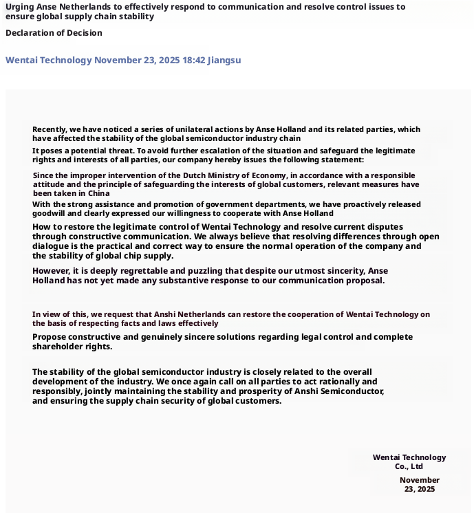
Blog posts of '2025' 'November'

A Real Risk Case in Component Kitting: Recent BGA Issues - Refurbishment, Contamination, and Failed Solderability!

A Real Risk Case in Component Kitting: Recent BGA Issues - Refurbishment, Contamination, and Failed Solderability!

Word Explanation

Solderability Test is a standardized method for evaluating the soldering performance of electronic components. By simulating actual soldering conditions (such as temperature, time, flux action, etc.), it observes the wetting of solder on the surface of pins or solder balls.
In electronic component inspection, the Solderability Test is often regarded as a "basic process", but for devices adopting BGA (Ball Grid Array) packaging, it is a crucial link in assessing reliability.
Today, through the problems found by Onepcba in the testing of BGA samples from different batches of customers' Component kitting recently, we will discuss the importance of solderability for BGA and why the Solderability Test is an indispensable testing link.
In the first batch of samples, inspectors found obvious contamination and scratches during the External Visual Inspection (EVI) phase.
Even without considering soldering performance, the contamination and scratches on the surface of BGA packaging themselves pose potential risks. Contaminants such as grease, dust, or ionic pollution from human contact may lead to increased leakage current or electrical short circuits; if scratches penetrate the metal layer or solder mask, they will damage the insulation protection.
For high-reliability industries such as automotive, aerospace, and medical, even if appearance abnormalities do not directly affect functionality, they may be regarded as signals of abnormalities in the manufacturing or supply chain processes.
At the same time, on the other side of the contamination and scratches, inspectors also found signs of refurbishment.
This means the device may have been used, removed, or exposed to an uncontrolled environment, and then re-entered the market after processes such as re-polishing, cleaning, or reballing.
Such refurbishment behaviors often damage the sealing performance and pad flatness of the original packaging, leading to internal structure damage or uneven heating of pins.
Even if the appearance is "restored", internal microcracks, residual contaminants, or metal fatigue may still cause early failure during use.
In another batch of BGA test samples, no signs of refurbishment or usage were found.
However, contamination was also found on the solder balls of these samples.
After entering the solderability test phase, a key problem was exposed: some solder balls exhibited poor wetting and insufficient solder spreading, and were ultimately judged as failed.
Failure in the solderability test indicates that the component pins or pads cannot form a reliable metal bond with the solder.
This is usually caused by oxidation, contamination, or plating aging.
Unlike traditional pin devices, all solder joints of BGA are located at the bottom of the chip, and they can hardly be directly observed with the naked eye after soldering is completed.
This means that once there are hidden dangers in solderability (such as solder ball oxidation, contamination, or deformation), it is likely to lead to the following during the assembly process:
  • Cold solder joints: The solder joints seem to be bonded, but there is actually poor contact;
  • Bubbles or voids: Reduce electrical conductivity and heat dissipation performance;
  • Early failure: Accelerated fracture under high temperature and high stress environments.
These risks often only manifest after the product is put into use, and the resulting rework, recall, or reputation loss far exceeds the testing cost.
Therefore, conducting solderability tests on BGA devices is not only necessary but also crucial.
In the case shared today, the Onepcba laboratory team combined multiple testing methods: External Visual Inspection (EVI) to find surface scratches, contamination, and signs of refurbishment; Solderability Test to verify the wetting of solder balls; and X-ray analysis to detect internal defects of solder balls.
Through comprehensive analysis, it can be judged whether the problem is caused by surface oxidation of some solder balls due to previous use and poor cleaning processes, resulting in insufficient wetting of the metal layer by the solder.
These findings helped the customer trace the problematic link and also reminded that the service requirements of Component kitting are: any slight negligence in storage, transportation, packaging, and even production line switching may lead to subsequent soldering failures.
BGA packaging represents the trend of high-density and high-performance electronic assembly, but it also places higher requirements on surface cleanliness and soldering process control.
With multi-dimensional testing capabilities covering solderability, appearance, X-ray, microscopic analysis, etc., Onepcba helps Component kitting identify risks from the source, ensuring that every link of the device from procurement to assembly is traceable, verifiable, and reliable.

About Us

Onepcba has an ISO17025-accredited laboratory, providing accurate and reliable professional testing. It can objectively and impartially test electronic components, providing true and reliable data and evaluation results for Component kitting buyers.
【Real-World Risk Case】 in Component Kitting: MOSFETs that passed both visual inspection and X-Ray failed completely in this test!
Recently, in Onepcba's service for client Component King, a comprehensive inspection was conducted on a batch of MOSFET components in accordance with the client's requirements. This batch passed both External Visual Inspection (EVI) and X-Ray inspection with no obvious physical abnormalities detected.
However, during the subsequent functional testing phase, 80 samples failed to meet the standards for two key indicators in the DC parameter test.
In the External Visual Inspection (EVI) process, inspectors confirmed that all samples featured clear surface markings, no visible scratches, deformation, re-marking, or re-grinding traces—fully complying with conventional qualification criteria.
X-Ray inspection similarly revealed intact internal structures, with normal bonding wires and chip placement, no voids, lead fractures, or obvious counterfeit characteristics, thus being deemed "Pass."
Nevertheless, during the functional testing (DC parameter test), each sample underwent standard DC parameter measurements. The results indicated that all 80 samples failed to meet the specified ranges for two critical
parameters: BVDSS (Breakdown Voltage, Drain-Source) and IDSS (Leakage Current, Drain-Source).
To clarify: What is DC parameter testing, and why is it crucial for MOSFETs?
DC parameter testing refers to the quantitative measurement of key electrical characteristics of MOSFETs under DC conditions, including:
  • VGS(th): Threshold Voltage
  • RDS(on): On-State Resistance
  • IDSS: Drain-Source Leakage Current
  • BVDSS: Drain-Source Breakdown Voltage
  • VSD: Diode Forward Voltage Drop, etc.
These parameters directly determine whether a MOSFET can properly turn on/off in a circuit, as well as its conduction loss and thermal performance under rated current.
Deviations from specified parameters can result in reduced efficiency and abnormal heating at best, or short circuits, breakdowns, or system failures at worst.
Many counterfeit, refurbished, or recycled MOSFETs exploit the limitation that "internal electrical degradation is difficult to detect via visual or X-Ray inspection." By means of grinding and re-marking, they are disguised as new components. Such parts often pass static inspections but fail during actual operation when powered on.
The test results for this batch of 80 MOSFETs demonstrate that External Visual Inspection + X-Ray inspection can only rule out obvious physical counterfeiting and structural defects, but cannot guarantee that the component's electrical performance meets specifications.
Functional testing—especially DC parameter testing—is the decisive step in verifying whether a MOSFET is truly usable and capable of stable operation. Omitting this step exposes the supply chain to significant potential risks.
Against the backdrop of a complex and volatile global supply chain, Component Kitting involves a vast array of component models. To address this, we have integrated a comprehensive inspection process for clients purchasing critical power devices: External Visual Inspection (EVI), X-Ray inspection, and functional testing (DC + AC parameters). If necessary, decapsulation analysis and failure analysis can be added.
Should you require inspection of existing inventory or new batches, please feel free to contact Onepcba's Component Kitting department. We will provide fast and professional support.
PCIe PCB Design Specifications! (Recommended for Bookmarking)

PCI-Express (Peripheral Component Interconnect Express) Design Specifications for PCB

PCI-Express (Peripheral Component Interconnect Express), formerly named "3GIO", is a high-speed serial computer expansion bus standard proposed by Intel in 2001. It aims to replace the legacy PCI, PCI-X, and AGP bus standards.
PCIe features high-speed serial point-to-point dual-channel transmission with dedicated bandwidth allocated to each connected device (no shared bus bandwidth). Key supported functions include active power management, error reporting, end-to-end reliable transmission, hot-swapping, and Quality of Service (QoS).
The following are the design specifications for PCIe PCBs:
  1. The trace length from the edge of the gold finger to the PCIe chip pins shall be limited to 4 inches (approximately 100mm).
  2. PCIe PERP/N, PETP/N, and PECKP/N are three differential pairs. Ensure proper isolation: maintain a 20mil spacing between differential pairs and between differential pairs and all non-PCIe signals to minimize harmful crosstalk and Electromagnetic Interference (EMI). Avoid high-frequency signals on the reverse side of the chip and PCIe signal traces; a full ground plane (GND) is recommended.
  3. The length difference between the two traces in a differential pair shall not exceed 5mil, with length matching required for every segment of the two traces. Use a 7mil trace width and 7mil spacing between the two traces in each differential pair.
  4. When PCIe signal pairs change layers, place ground vias near the signal vias—1 to 3 ground vias per signal pair are recommended. Use 25/14 vias for PCIe differential pairs, and the two vias must be symmetrically placed.
  5. PCIe requires AC coupling between the transmitter and receiver. The two AC coupling capacitors for a differential pair must have the same package size, be symmetrically placed, and located close to the gold finger. The recommended capacitance is 0.1μF, and through-hole packages are prohibited.
  6. Signals such as SCL shall not route through the PCIe main chip.       
Proper trace design enhances signal compatibility and reduces signal reflection and electromagnetic loss. PCIe bus signals use high-speed serial differential communication; therefore, adhering to the routing requirements and specifications for high-speed differential pairs is critical to ensuring reliable PCIe bus communication.
PCIe is a dual-simplex point-to-point serial differential low-voltage interconnect. Each lane consists of two differential signal pairs: transmit pair (Txp/Txn) and receive pair (Rxp/Rxn). These signals operate at 2.5 GHz with an embedded clock, which simplifies routing rules by eliminating length matching requirements across different differential pairs.
As PCIe serial bus transmission rates continue to increase, designing to minimize insertion loss and jitter budget becomes particularly important. In PCIe backplane design, the primary routing challenge lies in these differential pairs. Figure 1 illustrates key specifications for PCIe high-speed serial differential pair routing, including four common fan-in/fan-out configurations (labeled A, B, C, and D). Configuration A (symmetrical pin fan-in/fan-out) offers the best performance, followed by D, while B and C are viable alternatives. Below is a summary of key considerations for PCIe LVDS signal routing:
Figure 1: PCIe Differential Pair Routing Specifications
(1) For adapter cards or slots, the trace length from the gold finger edge/slot pins to the PCIe Switch pins shall not exceed 4 inches. Additionally, long-distance traces should be routed diagonally on the PCB.
(2) Avoid reference plane discontinuities such as splits and gaps.
(3) When LVDS signals change layers, ground vias must be placed close to the signal vias—at least 1 to 3 ground vias per signal pair are required. Never route traces across plane splits.
(4) Minimize trace bends to avoid introducing common-mode noise, which degrades differential pair signal integrity and increases EMI. All trace bends shall have an angle of ≥135 degrees. Maintain a spacing of ≥20mil between differential pair traces, and the minimum length of bent segments shall be ≥1.5 times the trace width.
When serpentine traces are used for length matching (as shown in Figure 2), each long bend segment must be at least 15mil (3 times the 5mil trace width). The maximum distance between serpentine bends and the other trace in the differential pair shall not exceed twice the normal differential pair spacing.
Figure 2: Serpentine Routing
(5) The length difference between the two data traces in a differential pair shall be within 5mil, with length matching required for every segment. Length matching should be implemented near the location of the length discrepancy (see Figure 3). Note that length matching is not required between transmit and receive pairs—only within individual differential pairs. A spacing of 5mil or 10mil is allowed in the fan-out area. Traces within 50mil do not require a reference plane. Length matching should be placed close to signal pins and achieved using small-angle bends.
Figure 3: PCIe Differential Pair Length Matching Design
To minimize length mismatch, the number of left bends should be as equal as possible to the number of right bends. When serpentine traces are used for length matching, each long bend segment must be ≥3 times the trace width. The maximum distance between serpentine bends and the other trace in the differential pair shall be ≤ twice the normal differential pair spacing. Additionally, when multiple bends are used for length matching to a single pin, the length of the unmatched segment shall be ≤45mil.
(6) PCIe requires AC coupling between the transmitter and receiver, with coupling capacitors typically placed close to the transmitter.
The two AC coupling capacitors for a differential pair must have the same capacitance value, package size, and symmetric placement. If possible, transmit differential pairs should be routed on the top layer. Capacitance values shall range from 75nF to 200nF, with 100nF preferred. Surface-mount device (SMD) packages such as 0402 are recommended; 0603 is acceptable, but through-hole packages are prohibited. The input and output traces of the capacitors for the two signals in a differential pair shall be symmetrical. Minimize trace separation during matching, and keep the length of traces separating the differential pair to the pins as short as possible.
 
Why are different test frequencies/voltages used to test the capacitance of capacitors, given their different capacitance ranges?

Why are different test frequencies/voltages used to test capacitance for different capacitance ranges?

The frequency setting of the instrument depends primarily on the parasitic components of the component. For more accurate component testing, the SRF (Self-Resonant Frequency) measurement frequency of the component should be avoided. Industry users set standards for different frequency points based on capacitance values ​​(Table 1). Capacitances above 10uF are considered within the tantalum capacitor range. Therefore, as the ceramic capacitance range begins to expand to the tantalum capacitor range, the industry applies the frequency standards for tantalum capacitor measurements to ceramic capacitors.

The applied voltage also depends on the capacitor's capacitance. Typically, a voltage of 1.0 ± 0.2 Vrms is applied for 10uF and below. However, for above 10uF, the applied voltage is 0.5 ± 0.2 Vrms. High-capacitance capacitors have extremely low impedance; therefore, to supply sufficient current for measurement, the power supply needs to provide more current than that supplied with 1.0 ± 0.2 Vrms. Therefore, by reducing the applied voltage, the power supply will be able to provide sufficient current to accurately measure high-capacitance capacitors.

Class Type Capacitance Frequency Voltage

Class I 1,000pF and under 1MHz ± 10% 0.5 ~ 5 Vrms Over 1,000pF 1kHz ± 10%

Class II 10uF and under 1kHz ± 10% 1.0 ± 0.2 Vrms Over 10uF 120Hz ± 20% 0.5 ± 0.2 Vrms

Nexperia 16474 models (MOS, transistors, ICs, IGBTs) , SPQ,MOQ and (COO) Certificate of Origin lookup

Nexperia 16474 models (MOS, transistors, ICs, IGBTs) , SPQ,MOQ and (COO) Certificate of Origin lookup

Nexperia 10911 diodes SPQ,MOQ and (COO) Certificate of Origin lookup

Nexperia 83 IGBTs and modules SPQ,MOQ and (COO) Certificate of Origin lookup

Nexperia 4244 logic ICs (74 series) SPQ,MOQ and (COO) Certificate of Origin lookup

Nexperia 1236 MOS (BUK series, etc.) SPQ,MOQ and (COO) Certificate of Origin lookup

This is an excerpt of the table starting with a model number; please download the attachment to view the complete data.

Nexperia 10911 diodes (COO) Certificate of Origin lookup
BL DescriptionBookpartSPQMOQLT WKSCOO
Bipolar Discretes1N4531,113100005000012China
Bipolar Discretes1N4531,133100005000012China
Bipolar Discretes1N4531,14350005000012China
Bipolar Discretes1N4728A,11350003000012China
Bipolar Discretes1N4728A,13350003000012China
Bipolar Discretes1N4729A,11350003000012China
Bipolar Discretes1N4729A,133500030000 China
Bipolar Discretes1N4730A,11350003000012China

etc.


Nexperia 83 IGBTs and modules (COO) Certificate of Origin lookup
BL DescriptionBookpartSPQMOQLT WKSCOO
Wide Band Gap IGBT and ModuleGAN039-650NBBHP100010008Philippines
Wide Band Gap IGBT and ModuleGAN039-650NTBJ1000100016Philippines
Wide Band Gap IGBT and ModuleGAN039-650NTBZ1000  Philippines
Wide Band Gap IGBT and ModuleGAN041-650WSBQ3003008China
Wide Band Gap IGBT and ModuleGAN063-650WSAQ300300 Philippines
Wide Band Gap IGBT and ModuleGAN080-650EBEZ250025008China
Wide Band Gap IGBT and ModuleGAN111-650WSBQ30030033China
Wide Band Gap IGBT and ModuleGAN140-650EBEZ250025008China


etc.


Nexperia 4244 logic ICs (74 series) (COO) Certificate of Origin lookup
BL DescriptionBookpartSPQMOQLT WKSCOO 
ICS74ABT00D,1182500250018China 
ICS74ABT00PW,1182500250018China 
ICS74ABT04D,1182500250014China 
ICS74ABT04PW,1182500250018China 
ICS74ABT08D,1182500250018China 
ICS74ABT08PW,1182500250018China 
ICS74ABT125BQ,1153000300016China 
ICS74ABT125D,6232500500018China 


etc.


Nexperia 1236 MOS (BUK series, etc.) (COO) Certificate of Origin lookup
BL DescriptionBookpartSPQMOQLT WKSCOO
MOS Discretes2N7002,21530004800014China
MOS Discretes2N7002,235100005000014China
MOS Discretes2N7002/HAMR30004800014China
MOS Discretes2N7002AKM-QYL100004000016China
MOS Discretes2N7002AK-QR30006900014China
MOS Discretes2N7002AKQB-QZ50001500012China
MOS Discretes2N7002AKRA-QZ50002000012China
MOS Discretes2N7002AKS-QX30002700014Malaysia

etc.

High quality aerospace circuit board disassembly using Xilinx chips

① On the circuit board, manually soldered joints can be seen connected to movable wires, but their ability to withstand repeated vibrations is definitely not as good as connectors (even those with leads)
② This is a space board that has already been put into use and was only dismantled later
③ It uses chips from Xilinx, which has been acquired by AMD and has become a subsidiary of AMD
④ What are the standards for aerospace circuit board levels? Have any industry partners shared them

Current humanoid robots have an intelligence equivalent to a one-year-old child, and they navigate amidst controversies surrounding remote control and counterfeiting.

Recently, images of humanoid robots running on the track and performing at exhibitions have gone viral. However, many observant viewers noticed that the engineers were still holding remote controls! The debate over whether "remote control equals fraud" is intensifying online and in the media. Today, we'll specifically discuss the issue of remote control of humanoid robots and fraud. Behind this lies a cognitive gap between technological progress and public expectations.

What is a one-year-old baby like? Robots are like that now.

Just like a one-year-old learning to walk, they need adults to support and protect them, and if they fall, they need to be picked up immediately. Humanoid robots are similar: they can take a few steps and pick things up on their own, but they rely on a "remote control" as an "invisible crutch." For example, when humanoid robots are trained in factories, they can perform tasks such as inspecting car door locks and affixing car stickers, but they must first go through the three steps of "perception-planning-execution." Autonomous decision-making in open environments is something the world hasn't yet mastered. An experienced worker in the industry gave an analogy: a robot's "cerebellum" can control balance and joint movement, but its "brain" gets confused when faced with complex situations—just like a baby can imitate walking, but is prone to falling if not being led by an adult.

Remote control isn't fraud; it's a "learning tool" for growth.

Some say "using remote control is deception," but Academician Han Guangjie said that remote control is more like an "emergency button," allowing engineers to take over and ensure safety when the robot suddenly becomes confused. Whether humanoid robot manufacturers are fraudulent depends on their advertising. If they claim "fully autonomous" operation while relying on remote control, that's fraud. If they're honest and the remote control is a "learning tool" during development, like a parent helping a toddler learn to walk, that's the proper approach. Think about it: robots learn skills through "imitation-practice-autonomy." Tesla's Optimus and Zhiyuan Yuanzheng A2 do this, collecting data through human "hands-on" teaching to form an evolutionary loop of "teaching-training-autonomy." This isn't technological regression; it's an essential part of growth.

From "learning to walk at one year old" to "walking independently," there are still hurdles to overcome.

Humanoid robots need to overcome several obstacles to walk independently without a remote control. Firstly, technically, the A2 robot from Zhiyuan Robotics, capable of traversing 100 kilometers across provinces, relies on multi-sensor fusion of dual GPS, LiDAR, and infrared depth cameras. While it can recognize complex terrain and avoid crowds, it is prone to misjudging situations and requires alerts. Secondly, in terms of safety, human-robot mixed environments require safety measures. For example, CloudMinds uses a cloud-based brain system to ensure remote intervention when robots make mistakes. Thirdly, in terms of industry, humanoid robots entering factory workshops must first overcome challenges such as cross-scene migration and small-sample learning. Currently, the robotics industry is moving towards "Level 3," aiming to handle most scenarios autonomously and only call for human assistance in complex situations. Experts predict that achieving fully autonomous "Level 4 and Level 5" robots will require another 3-5 years of development.

Controversy is a wake-up call, but also an opportunity.

This debate has also served as a reminder to the industry: technology must allow for trial and error, but communication must be transparent. Manufacturers must be honest and not mislead with claims of "fully autonomous" technology; the public must also understand that new technologies, like toddlers learning to walk, need room to grow. With breakthroughs in technologies like multimodal perception and reinforcement learning, humanoid robots will eventually need to "retire" once they reach 5 or 6 years old. Currently, robots are in a critical "learning-to-walk" stage. Controversy isn't a bad thing; it forces the industry to become more standardized. Technology hasn't been idle either, constantly pushing forward. As Pang Jianxin said, the development of humanoid robots will take three steps: first, performing limited tasks in structured scenarios; second, learning to accompany and interact; and finally, entering the home. Currently, UBTECH's training at Geely's factory and the A2 robot's cross-province journey are both examples of "learning to walk." When robots can, as Lu Junguo said, accompany the elderly and care for children in the home, that will be true "independence."


The process of a robot learning to walk is similar to that of a toddler learning to walk. First, it needs support to walk, then it gradually learns to walk independently. It can't be rushed, and it can't be faked. Don't you agree? If we are more patient and accept its "dependency" like we do with a toddler learning to walk, and if companies focus on solid research and development, robots will eventually be able to "run" on their own, entering factories, shopping malls, and even our homes.


As we all know, the design of humanoid robots is in full swing in both China and the United States. So, what chips are used in China's humanoid robots?

Chips used in humanoid robots designed in China are functionally classified into core categories covering critical links such as decision-making, motion control, and perception. Key mainstream models are detailed below:

AI Decision-Making Chips (The "Brain")

  • International: NVIDIA Jetson Orin, Jetson AGX Thor.
  • Chinese Brands: Rockchip RK3588, Horizon Robotics Journey A2000 (Huashan Series), among others, are making significant strides in this sector.

Motion Control Chips (The "Cerebellum")

  • International: Texas Instruments (TI, U.S.) TMS320F28377D, STMicroelectronics (ST, Europe) STM32H7 series are widely adopted.
  • Chinese Brands: HPMicro HPM6E00, GigaDevice GD32H75E, etc., meet the microsecond-level synchronous control requirements for multi-joint systems.

Visual Sensing Chips (The "Eyes")

  • International: Sony (Japan) IMX series are common 2D vision CMOS chips.
  • Chinese Brands: Orbbec Femto series iToF chips, OmniVision (China) global shutter image sensors, enabling high-precision 3D perception and dynamic image capture.

Communication Interface Chips (The "Data Neural Network")

  • International: NXP S32K39, Infineon LAN9252 are widely used.
  • Chinese Brands: Create Bright Technology EtherCAT slave control chips, Youtai Micro low-latency Ethernet chips, adapting to high-real-time transmission needs.

Power Management Chips (The "Energy Heart")

  • International: Texas Instruments (TI, U.S.) BQ27546, Analog Devices (ADI) LTC3880 dominate the market.
  • Chinese Brands: Eastchip Semiconductor DK87XXBD series, SGMICRO high-precision power management chips, suitable for wide-voltage and fast-charging scenarios.

Memory Chips (The "Memory Center")

  • Chinese Brand: GigaDevice SPI NOR Flash GD25LX series, with a data throughput of 400MB/s, can meet the requirements of fast robot code reading and program startup.              
Analysis of the Duration of the Market Price Increase Cycle for the Popular Component MT53E512M32D1ZW-046 WT:B1
 What to do when customers are always a step behind the market?

Last week, a friend who dabbles in the memory storage market mentioned that he believes prices in the storage market always exhibit a time-lag effect. For instance, for a certain component: in the first week, when he quoted 5 US dollars, the customer only accepted 3 US dollars; in the second week, when he quoted 8 US dollars, the customer agreed to 5 US dollars; by the third week, when he offered 12 US dollars, the customer was willing to accept 8 US dollars... In fact, this scenario indicates that the component is in an upward price cycle. Today's peak becomes tomorrow's low. Take the MT53E512M32D1ZW-046 WT:B1 as shown —its "tearful sale price" at the end of October turned out to be a "steal" in mid-November. In just three weeks, the price nearly tripled, and by last weekend, quotes for this component had reached 30 US dollars.
So what's the allure of trading components in such upward price cycles? It lies in locking in orders when the price is between 1 and 9 (on a hypothetical scale), say at 3 or 4, then selling when it climbs to 7 or 8. Within just two to three weeks, you can secure a price difference of two to three times, or even more. This is the reason why stockpilers are so drawn to this practice.
Of course, it’s crucial to analyze data carefully and avoid overcommitting during downward price cycles. As for the critical turning point of this round of ups and downs in the storage market, current comprehensive market assessments—combined with the explosive news of ChangXin Memory Technology launching DDR5 (which may effectively deter further fires at certain foreign storage factories)—have led some players to predict that this storage market rally may last until April-June next year (market information is for reference only and not an authoritative conclusion).
In fact, this phenomenon isn’t unique to the storage sector; many practices in the broader IC (Integrated Circuit) industry follow a similar pattern. For example, during the upward price cycles of ADI and Nexperia this year, it was common for channels and suppliers to engage in order flipping and price hikes. Seasoned players would choose to collaborate closely with channels to profit together; otherwise, they’d be merely acting as intermediaries relying solely on industry connections. However, acting as an intermediary is particularly challenging in the storage market, as it requires significantly larger capital investment. Many small and micro IC intermediaries simply lack the financial capacity to participate—this is why you may watch the memory market soar daily but struggle to enter it.


('Carrying baskets'is the image of the public's'reverse trading'of traders
Statement-It is like "carrying a basket"to transfer goods between different markets andentities,without directly creating physical value(such as production and research anddevelopment),but by identifying and capturing opportunities for supply-demand mismatch,achieving short-term transfer of ownership of goods and making profits.
In academic contexts,similar concepts include "middlemanarbitrage,""speculative trading,"and "spread trading
Trading),But 'basket lifting'emphasizes more on operationalflexibility and asset light attributes(no need for self ownedwarehouses or production lines,relying on funds and channels).

Wingtech Technology Co., Ltd. Responds Strongly! New Statement on Nexperia Netherlands Issues
On November 23rd, Wingtech Technology released the "Statement Urging Nexperia Netherlands to Earnestly Respond to Communications and Resolve the Control Right Issue to Safeguard the Stability of the Global Supply Chain" on its official WeChat public account.

Statement Urging Nexperia Netherlands to Earnestly Respond to Communications and Resolve the Control Right Issue to Safeguard the Stability of the Global Supply Chain

Wingtech TechnologyNovember 23rd, 2025 18:42 JiangsuRecently, we have noticed a series of unilateral actions by Nexperia Netherlands and its related parties, which have posed potential threats to the stability of the global semiconductor industry chain. To prevent the situation from further escalating and safeguard the legitimate rights and interests of all parties, our company hereby issues the following statement:Since the improper intervention by the Dutch Ministry of Economic Affairs, adhering to the principle of responsibility and safeguarding the interests of global customers, with the strong assistance and promotion of relevant Chinese government departments, we have taken the initiative to show goodwill and clearly expressed our willingness to conduct constructive communications with Nexperia Netherlands on how to restore Wingtech Technology's legitimate control rights and properly resolve the current disputes. We have always believed that resolving differences through candid dialogue is a practical and correct approach to ensuring the normal operation of the company and the stability of global chip supply.However, it is deeply regrettable and puzzling that despite our utmost sincerity, Nexperia Netherlands has so far not made any substantive response to our communication proposals.In view of this, we request Nexperia Netherlands to put forward constructive and truly sincere solutions on how to restore Wingtech Technology's legitimate control rights and complete shareholder rights on the basis of earnestly respecting facts and laws.The stability of the global semiconductor industry is crucial to the overall development of the industry. We once again call on all parties to act in a rational and responsible manner, jointly safeguard the stability and prosperity of Nexperia Semiconductor, and ensure the supply chain security of global customers.Wingtech Technology Co., Ltd.November 23rd, 2025
Source: Wingtech Technology's official WeChat public account
This is Wingtech Technology's third official statement since the Netherlands announced on November 19th that it had "suspended its intervention in Nexperia Semiconductor". The specific content and timeline are as follows:
On November 19th, Wingtech Technology released the "Progress Report on the Operation and Management of Subsidiaries". The announcement stated that the ministerial order suspended as referred to in the statement by the Minister of Economic Affairs and Climate Policy of the Netherlands is the order issued by the Ministry of Economic Affairs and Climate Policy of the Netherlands to Nexperia on September 30th, 2025 (Netherlands time). This ministerial order requires Nexperia and all its global 30 entities including subsidiaries, branches, and offices to refrain from making any adjustments to their assets, intellectual property rights, businesses, and personnel, with a validity period of one year.
Although the aforementioned ministerial order has been announced as suspended, the emergency measures ruled by the Enterprise Court on October 7th, 2025 (Netherlands time) remain in effect and have not been affected by the suspended ministerial order in any way. All emergency measures of the Enterprise Court as explained in the company's announcement on October 13th are still ongoing, and the company's control over Nexperia is still restricted. Investors are advised to pay attention to investment risks.
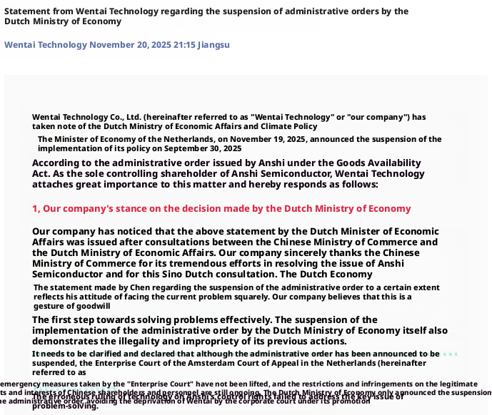
On November 20th, Wingtech Technology released the "Statement by Wingtech Technology on the Suspension of the Administrative Order by the Dutch Ministry of Economic Affairs" on its official WeChat public account. The statement pointed out that although the administrative order has been announced as suspended, the emergency measures issued by the Enterprise Court of the Amsterdam Court of Appeal in the Netherlands have not been lifted. The Dutch Ministry of Economic Affairs is obligated to thoroughly and comprehensively resolve the Nexperia Semiconductor issue, and Wingtech Technology's complete rights as a shareholder and its legitimate control over Nexperia must be restored.

Statement by Wingtech Technology on the Suspension of the Administrative Order by the Dutch Ministry of Economic Affairs

Wingtech TechnologyNovember 20th, 2025 21:15 JiangsuWingtech Technology Co., Ltd. (hereinafter referred to as "Wingtech Technology" or "our company") has noticed the statement issued by the Minister of Economic Affairs and Climate Policy of the Netherlands (hereinafter referred to as "the Dutch Ministry of Economic Affairs") on November 19th, 2025, stating that it has "suspended the implementation of the administrative order issued to Nexperia on September 30th, 2025 in accordance with the Goods Availability Act". As the sole controlling shareholder of Nexperia Semiconductor, Wingtech Technology attaches great importance to this and hereby makes the following response regarding relevant matters:

I. Our Company's Position on the Decision of the Dutch Ministry of Economic Affairs

We have noticed that the above-mentioned statement by the Dutch Minister of Economic Affairs was issued after consultations between the Ministry of Commerce of the People's Republic of China and the Dutch Ministry of Economic Affairs. We sincerely thank the Ministry of Commerce of the People's Republic of China for its tremendous efforts in resolving the Nexperia Semiconductor issue and the current China-Netherlands consultations. The Dutch Minister of Economic Affairs' expression of suspending the administrative order reflects to a certain extent its attitude of facing up to the current problem, which we believe is the first step towards properly resolving the issue. The Dutch Ministry of Economic Affairs' suspension of the administrative order itself also indicates the illegality and impropriety of its previous actions.
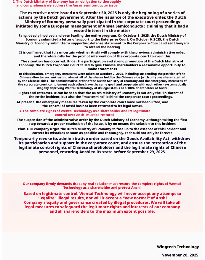
It should be clarified and stated that although the administrative order has been announced as suspended, the emergency measures issued by the Enterprise Court of the Amsterdam Court of Appeal in the Netherlands (hereinafter referred to as "the Enterprise Court") have not been lifted. The restrictions and infringements on the legitimate rights and interests of Chinese shareholders and personnel are still ongoing. The Dutch Ministry of Economic Affairs only announced the suspension of the administrative order, evading the erroneous ruling of the Enterprise Court, which was promoted by it, to deprive Wingtech Technology of control over Nexperia, and failed to address the key to solving the problem.

II. The Dutch Ministry of Economic Affairs is Obligated to Thoroughly and Comprehensively Resolve the Nexperia Semiconductor Issue

The administrative order issued on September 30th, 2025 is only the beginning of a series of actions by the Dutch government. After the issuance of the administrative order, the Dutch Ministry of Economic Affairs personally participated in the Enterprise Court proceedings initiated by some European management of Nexperia Semiconductor, claimed itself as an interested party, and deeply participated in and even dominated the entire process. On October 1st, 2025, the Dutch Ministry of Economic Affairs submitted a letter of support to the Enterprise Court; on October 6th, 2025, it submitted supporting defense statements to the Enterprise Court and sent lawyers to attend the hearing, clearly stating that it could not determine whether Nexperia would comply with the previous administrative order, thus calling for "the rapid intervention of the Enterprise Court to avoid this situation". With the participation and strong promotion of the Dutch Ministry of Economic Affairs, the Dutch Enterprise Court, without giving Chinese shareholders a reasonable opportunity to present their cases, arbitrarily made emergency measures on October 7th, 2025, such as suspending the positions of Chinese directors and placing almost all shares held by Chinese parties in custody (with Chinese parties retaining only 1 share). The administrative order of the Dutch Ministry of Economic Affairs and the emergency measures of the Enterprise Court are complementary in means, consistent in goals, and coordinate with each other—systematically and illegally depriving Wingtech Technology of its legitimate rights and interests as the 100% shareholder of Nexperia. It is evident that the Dutch Ministry of Economic Affairs is not only the "initiator" of the entire incident but also the "behind-the-scenes pusher" of the Enterprise Court proceedings.
At present, the emergency measures issued by the Enterprise Court have not been lifted, and the control of Nexperia has not been returned to its legitimate owner.

III. Wingtech Technology's Complete Rights as a Shareholder and Its Legitimate Control Over Nexperia Must Be Restored

Although the Dutch Ministry of Economic Affairs' decision to suspend the administrative order is the first step towards properly resolving the issue, it is by no means a solution to this incident. We urge the Dutch Ministry of Economic Affairs to face up to the essence of this incident and correct its mistakes as soon as possible and thoroughly. It should not only permanently revoke the administrative order issued based on the Goods Availability Act and withdraw its participation in and support for the Enterprise Court but also ensure that the legitimate control rights of Chinese shareholders and the legitimate rights of Chinese personnel are restored, and Nexperia is returned to the state before September 29th, 2025.
We firmly demand that any true solution must be based on restoring Wingtech Technology's complete rights as a shareholder and its legitimate control over Nexperia. Wingtech Technology will never accept any attempt to "legalize" illegal results, nor will it accept a "new normal" of Nexperia's equity and governance created through illegal procedures. We will take all legal means to maximize the protection of the legitimate rights and interests of our company and all shareholders.
Wingtech TechnologyNovember 20th, 2025
Source: Wingtech Technology's official WeChat public account
On November 23rd, Wingtech Technology released the "Statement Urging Nexperia Netherlands to Earnestly Respond to Communications and Resolve the Control Right Issue to Safeguard the Stability of the Global Supply Chain" on its official WeChat public account.
The statement said that the company has noticed a series of unilateral actions by Nexperia Netherlands and its related parties, which have posed potential threats to the stability of the global semiconductor industry chain.
"It is deeply regrettable and puzzling that despite our utmost sincerity, Nexperia Netherlands has so far not made any substantive response to our communication proposals," the statement said. In the statement, Wingtech Technology requested Nexperia Netherlands to put forward constructive and truly sincere solutions on how to restore Wingtech Technology's legitimate control rights and complete shareholder rights on the basis of respecting facts and laws.
The following is a collation of information recently released by some official and authoritative media since the occurrence of the Nexperia incident:
On November 1st, China announced exemptions for eligible exports of Nexperia Semiconductor.
On November 2nd, Nexperia China issued an announcement letter to customers stating that Nexperia Netherlands unilaterally decided to stop supplying wafers to the packaging and testing factory (ATGD) located in Dongguan starting from October 26th, 2025.
On November 7th (local time), the Dutch government stated that China will soon resume chip supply.
On November 8th, China agreed to the request of the Dutch Ministry of Economic Affairs to send personnel to China for consultations.
On November 13th, Jiemian News reported that according to automotive industry officials, Nexperia Semiconductor's Dutch branch has not been transporting silicon wafers to its Chinese subsidiary for assembly.
On November 13th, Dutch Minister of Economic Affairs Karelmans stated in an interview with The Guardian that he had "no regrets" about the Netherlands' decision to take over Nexperia on September 30th.
On November 14th, the Dutch Minister of Economic Affairs stated that a Dutch government delegation will travel to China "early next week" to seek a solution to the issue regarding Nexperia Semiconductor, a subsidiary of Chinese company Wingtech Technology.
On November 14th, the Ministry of Commerce responded to Karelmans' remarks in the interview: China expressed extreme disappointment and strong dissatisfaction with such remarks that confuse right and wrong, reverse black and white, and act arbitrarily. The Dutch Ministry of Economic Affairs declined to comment on the same day.
On November 17th (local time), DutchNews reported that a Dutch delegation is visiting China this week.
On November 19th, Dutch Minister of Economic Affairs Karelmans issued a statement on social media platform X, stating that he had "suspended intervention in Nexperia Semiconductor".
On November 19th, Wingtech Technology announced that the company's control over Nexperia is still restricted.
On November 19th, the Ministry of Commerce: China welcomes the Netherlands' initiative to suspend the administrative order on Nexperia Semiconductor, believing it is the first step in the right direction towards properly resolving the issue, but there is still a gap from addressing the root cause of the turbulence and chaos in the global semiconductor production and supply chain.
In addition, the wafer issue has not yet been resolved.
[Case Study] The Secret in the Crack: A Metallographic Analysis of a Varistor!

OnePcba conducted a full-process incoming inspection on a varistor in accordance with customer requirements. In addition to routine appearance screening, the laboratory focused on "anatomical" structural verification through Cross Section (section analysis) to accurately check the integrity of the internal structure of the component.

Section analysis is a core technology for micro-detection of electronic components: through steps such as resin encapsulation curing, precision grinding, and mirror polishing, the internal structure details are finally presented intuitively with a metallographic microscope (magnification 50~500x). Its advantage lies in capturing tiny defects that cannot be identified by the naked eye and conventional detection.

For varistors, the "safety valves" of circuits, the significance of section detection is particularly critical. As the core of voltage protection in scenarios such as automotive electronics and power modules, even micron-level cracks, bubbles, or voids inside them may become "invisible bombs" for electrical breakdown and functional failure.


The test results showed that multiple samples had obvious crack and void defects, and the specific risk mechanisms are as follows:

  • Crack defects: Mainly caused by sintering stress in the production process, mechanical impact during transportation, or thermal stress caused by temperature fluctuations. Under high-voltage surge scenarios, arc discharge and local overheating are prone to occur at cracks, which may轻则 cause resistor functional failure, and重则 trigger circuit short circuits, threatening the safety of subsequent equipment.
  • Void defects: Mostly caused by uneven shrinkage of resin materials during packaging and gas residue during curing. Voids will reduce local heat dissipation efficiency and cause electric field concentration effect, which accelerates device aging under repeated voltage shocks and significantly shortens service life.

In fields such as automotive electronics (e.g., BMS battery management systems, radar sensors) and medical electronics that require "zero tolerance" for reliability, such potential defects are completely unacceptable. Once the device fails, it may cause serious consequences such as vehicle safety failures and medical equipment shutdowns.

This case profoundly reveals that the reliability of electronic components has never been a "number game on the parameter table", but a quality core hidden in the microstructure.

Every section analysis is an in-depth diagnosis of the "health status" of components; every test report of OnePcba is a quality protection wall built for the customer's supply chain. In the follow-up, we will continue to share special detection points of other components such as capacitors and chips, so stay tuned.