- upload bom file
- +86 0755-82770375
- info@onepcba.com
- Compare Products
- Change Location:
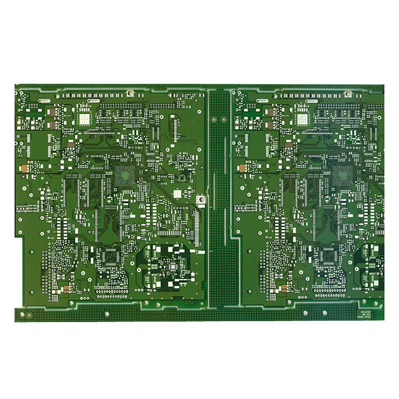
32-layer Multilayer PCB
Layer: 32
Thickness: 6 mm
Material: KB 6160
Copper: Outer 2 OZ, Inner 3 OZ
Surface: ENIG 3U
Application: Communication
Minimum hole: 0.15mm
Minimum line width: 3.1mil
Line spacing: 3.6mil
Product Details
Electronic design is trying to reduce its size while continuously improving the overall performance. Among small portable products from mobile phones to smart weapons, “small” is an eternal pursuit. High density integration (HDI) technology can make the terminal product design smaller, while also meeting higher standards of electronic performance and efficiency. At present, HDI is widely used in digital products, such as mobile phones, digital (camera) cameras, MP3, MP4, laptops, automotive electronics, etc. Mobile phones are the most widely used. HDI boards are usually manufactured by the Build up method. The higher the number of layers, the higher the technical level of the boards. General HDI boards are basically stacked once. High order HDI adopts advanced PCB technologies such as stacking technology, hole stacking, electroplating and hole filling, and laser direct drilling, etc. High order HDI boards are mainly used in 3G mobile phones, digital cameras, IC carriers, etc.