Recently, in Onepcba's service for client Component King, a comprehensive inspection was conducted on a batch of MOSFET components in accordance with the client's requirements. This batch passed both External Visual Inspection (EVI) and X-Ray inspection with no obvious physical abnormalities detected.
However, during the subsequent functional testing phase, 80 samples failed to meet the standards for two key indicators in the DC parameter test.
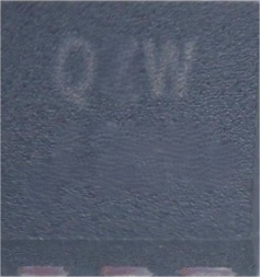
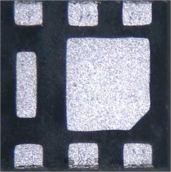
In the External Visual Inspection (EVI) process, inspectors confirmed that all samples featured clear surface markings, no visible scratches, deformation, re-marking, or re-grinding traces—fully complying with conventional qualification criteria.
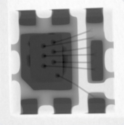
X-Ray inspection similarly revealed intact internal structures, with normal bonding wires and chip placement, no voids, lead fractures, or obvious counterfeit characteristics, thus being deemed "Pass."
Nevertheless, during the functional testing (DC parameter test), each sample underwent standard DC parameter measurements. The results indicated that all 80 samples failed to meet the specified ranges for two critical
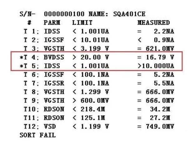
parameters: BVDSS (Breakdown Voltage, Drain-Source) and IDSS (Leakage Current, Drain-Source).
To clarify: What is DC parameter testing, and why is it crucial for MOSFETs?
DC parameter testing refers to the quantitative measurement of key electrical characteristics of MOSFETs under DC conditions, including:
- VGS(th): Threshold Voltage
- RDS(on): On-State Resistance
- IDSS: Drain-Source Leakage Current
- BVDSS: Drain-Source Breakdown Voltage
- VSD: Diode Forward Voltage Drop, etc.
These parameters directly determine whether a MOSFET can properly turn on/off in a circuit, as well as its conduction loss and thermal performance under rated current.
Deviations from specified parameters can result in reduced efficiency and abnormal heating at best, or short circuits, breakdowns, or system failures at worst.
Many counterfeit, refurbished, or recycled MOSFETs exploit the limitation that "internal electrical degradation is difficult to detect via visual or X-Ray inspection." By means of grinding and re-marking, they are disguised as new components. Such parts often pass static inspections but fail during actual operation when powered on.
The test results for this batch of 80 MOSFETs demonstrate that External Visual Inspection + X-Ray inspection can only rule out obvious physical counterfeiting and structural defects, but cannot guarantee that the component's electrical performance meets specifications.
Functional testing—especially DC parameter testing—is the decisive step in verifying whether a MOSFET is truly usable and capable of stable operation. Omitting this step exposes the supply chain to significant potential risks.
Against the backdrop of a complex and volatile global supply chain, Component Kitting involves a vast array of component models. To address this, we have integrated a comprehensive inspection process for clients purchasing critical power devices: External Visual Inspection (EVI), X-Ray inspection, and functional testing (DC + AC parameters). If necessary, decapsulation analysis and failure analysis can be added.
Should you require inspection of existing inventory or new batches, please feel free to contact Onepcba's Component Kitting department. We will provide fast and professional support.